SBOS671D September 2018 – December 2022 OPA2828 , OPA828
PRODUCTION DATA
- 1 Features
- 2 Applications
- 3 Description
- 4 Revision History
- 5 Pin Configuration and Functions
- 6 Specifications
-
7 Detailed Description
- 7.1 Overview
- 7.2 Functional Block Diagram
- 7.3
Feature Description
- 7.3.1 Phase-Reversal Protection
- 7.3.2 Electrical Overstress
- 7.3.3 MUX Friendly Inputs
- 7.3.4 Overload Power Limiter
- 7.3.5 Noise Performance
- 7.3.6 Capacitive Load and Stability
- 7.3.7 Settling Time
- 7.3.8 Slew Rate
- 7.3.9 Full-Power Bandwidth
- 7.3.10 Small-Signal Response
- 7.3.11 Thermal Shutdown
- 7.3.12 Low Offset Voltage Drift
- 7.3.13 Overload Recovery
- 7.4 Device Functional Modes
- 8 Application and Implementation
- 9 Device and Documentation Support
- 10Mechanical, Packaging, and Orderable Information
Package Options
Mechanical Data (Package|Pins)
Thermal pad, mechanical data (Package|Pins)
- DGN|8
Orderable Information
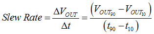
7.3.8 Slew Rate
The parameter of an amplifier that best describes the large-signal dynamic behavior is the slew rate. Slew rate is a measure of the maximum rate of change of the output voltage with respect to time, and is generally expressed in units of volts-per-microsecond, (V/µs). Typically, the slew rate is measured as the time for the output to swing from 10% of the final value to 90% of the final value. The slew rate for the signal illustrated in Figure 7-10 is given by Equation 3.
The slew rate of an amplifier is limited by the internal architecture of the amplifier, the amplifier quiescent power and internal capacitances. The OPAx828 maximize the slew rate by incorporating a slew-boost circuit. The proprietary slew boost circuit used in the OPAx828 results in a very high slew rate while maintaining low quiescent power levels. The internal slew boost circuit measures the input differential voltage present between the +IN and –IN input pins. If this input differential voltage is sufficiently large enough, the internal slew-boost circuit increases the internal biasing currents of the amplifier, thereby increasing the ability of the output to slew faster. To provide optimal dynamic performance, place power-supply bypass capacitors close to the OPAx828.
If the inputs of the amplifier have a large static or dc differential voltage present, the OPAx828 recognize that condition; not as an indicator of the need to slew faster, but rather as an overload condition. In this case, the OPAx828 internal biasing currents do not increase, and the quiescent current remains unchanged from normal operation.