SBOS891C October   2018  – September 2023 TMP144

PRODUCTION DATA  

  1.   1
  2. Features
  3. Applications
  4. Description
  5. Revision History
  6. Pin Configuration and Functions
  7. Specifications
    1. 6.1 Absolute Maximum Ratings
    2. 6.2 ESD Ratings
    3. 6.3 Recommended Operating Conditions
    4. 6.4 Thermal Information
    5. 6.5 Electrical Characteristics
    6. 6.6 UART Interface Timing
    7. 6.7 Timing Diagrams
    8. 6.8 Typical Characteristics
  8. Detailed Description
    1. 7.1 Overview
    2. 7.2 Functional Block Diagram
    3. 7.3 Feature Description
      1. 7.3.1 Power Up
      2. 7.3.2 Digital Temperature Output
      3. 7.3.3 Timeout Function
    4. 7.4 Device Functional Modes
      1. 7.4.1 Continuous Conversion Mode
      2. 7.4.2 Shutdown Mode
      3. 7.4.3 One-Shot Mode
      4. 7.4.4 Extended Temperature Mode
      5. 7.4.5 Temperature Alert Function
      6. 7.4.6 Interrupt Functionality
    5. 7.5 SMAART Wire / UART Interface
      1. 7.5.1 Communication Protocol
      2. 7.5.2 Global Software Reset
      3. 7.5.3 Global Initialization and Address Assignment Sequence
      4. 7.5.4 Global Clear Interrupt
      5. 7.5.5 Global Read and Write
      6. 7.5.6 Individual Read and Write
    6. 7.6 Register Maps
      1. 7.6.1 Temperature Result Register (P[1:0] = 00) [reset = 0000h]
      2. 7.6.2 Configuration Register (P[1:0] = 01) [reset = 0200h]
      3. 7.6.3 Temperature Low Limit Register (P[1:0] = 10) [reset = F600h]
      4. 7.6.4 Temperature High Limit Register (P[1:0] = 11) [reset = 3C00h]
  9. Application and Implementation
    1. 8.1 Application Information
    2. 8.2 Typical Application
      1. 8.2.1 Design Requirements
      2. 8.2.2 Detailed Design Procedure
        1. 8.2.2.1 Trace Length
        2. 8.2.2.2 Voltage Drop Effect
        3. 8.2.2.3 Power Supply Noise Filtering
      3. 8.2.3 Application Curves
    3. 8.3 Power Supply Recommendations
    4. 8.4 Layout
      1. 8.4.1 Layout Guidelines
      2. 8.4.2 Layout Example
  10. Device and Documentation Support
    1. 9.1 Device Support
      1. 9.1.1 Device Nomenclature
    2. 9.2 Receiving Notification of Documentation Updates
    3. 9.3 Support Resources
    4. 9.4 Trademarks
    5. 9.5 Electrostatic Discharge Caution
    6. 9.6 Glossary
  11. 10Mechanical, Packaging, and Orderable Information

Package Options

Refer to the PDF data sheet for device specific package drawings

Mechanical Data (Package|Pins)
  • YBK|4
  • YFF|4
  • YMT|4
Thermal pad, mechanical data (Package|Pins)
Orderable Information

Register Maps

Figure 7-17 shows the internal register structure of the TMP144. Communications between the registers are transferred through the interface in LSB-first order. The 8-bit command register as shown in , is used to determine the address pointer for the register that the host device wants to access.
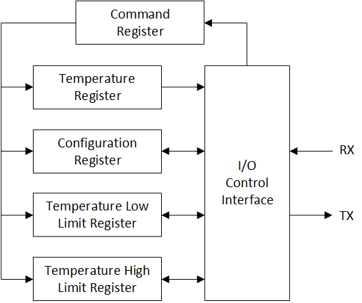
GUID-20200819-CA0I-SN0V-PLKL-JQXFWXGTPGLW-low.gifFigure 7-17 Internal Register Structure.

Table 7-4 Register Map
ADDRESS POINTER P[1:0]TYPERESETACRONYMREGISTER NAMESECTION
00R0000hTemp_ResultTemperature result registerGo
01R/W0200hConfigurationConfiguration RegisterGo
10R/W3C00hTlow_limitTemperature low limit registerGo
11R/WF600hThigh_limitTemperature high limit registerGo

Table 7-5 Register Section/Block Access Type Codes
Access TypeCodeDescription
Read Type
RRRead
RCRRead
Cto Clear
R-0R Read
-0Returns 0s
Write Type
WWWrite
W0CPW W
0C0 to clear
PRequires privileged access
Reset or Default Value
-nValue after reset or the default value