SBOS891C October   2018  – September 2023 TMP144

PRODUCTION DATA  

  1.   1
  2. Features
  3. Applications
  4. Description
  5. Revision History
  6. Pin Configuration and Functions
  7. Specifications
    1. 6.1 Absolute Maximum Ratings
    2. 6.2 ESD Ratings
    3. 6.3 Recommended Operating Conditions
    4. 6.4 Thermal Information
    5. 6.5 Electrical Characteristics
    6. 6.6 UART Interface Timing
    7. 6.7 Timing Diagrams
    8. 6.8 Typical Characteristics
  8. Detailed Description
    1. 7.1 Overview
    2. 7.2 Functional Block Diagram
    3. 7.3 Feature Description
      1. 7.3.1 Power Up
      2. 7.3.2 Digital Temperature Output
      3. 7.3.3 Timeout Function
    4. 7.4 Device Functional Modes
      1. 7.4.1 Continuous Conversion Mode
      2. 7.4.2 Shutdown Mode
      3. 7.4.3 One-Shot Mode
      4. 7.4.4 Extended Temperature Mode
      5. 7.4.5 Temperature Alert Function
      6. 7.4.6 Interrupt Functionality
    5. 7.5 SMAART Wire / UART Interface
      1. 7.5.1 Communication Protocol
      2. 7.5.2 Global Software Reset
      3. 7.5.3 Global Initialization and Address Assignment Sequence
      4. 7.5.4 Global Clear Interrupt
      5. 7.5.5 Global Read and Write
      6. 7.5.6 Individual Read and Write
    6. 7.6 Register Maps
      1. 7.6.1 Temperature Result Register (P[1:0] = 00) [reset = 0000h]
      2. 7.6.2 Configuration Register (P[1:0] = 01) [reset = 0200h]
      3. 7.6.3 Temperature Low Limit Register (P[1:0] = 10) [reset = F600h]
      4. 7.6.4 Temperature High Limit Register (P[1:0] = 11) [reset = 3C00h]
  9. Application and Implementation
    1. 8.1 Application Information
    2. 8.2 Typical Application
      1. 8.2.1 Design Requirements
      2. 8.2.2 Detailed Design Procedure
        1. 8.2.2.1 Trace Length
        2. 8.2.2.2 Voltage Drop Effect
        3. 8.2.2.3 Power Supply Noise Filtering
      3. 8.2.3 Application Curves
    3. 8.3 Power Supply Recommendations
    4. 8.4 Layout
      1. 8.4.1 Layout Guidelines
      2. 8.4.2 Layout Example
  10. Device and Documentation Support
    1. 9.1 Device Support
      1. 9.1.1 Device Nomenclature
    2. 9.2 Receiving Notification of Documentation Updates
    3. 9.3 Support Resources
    4. 9.4 Trademarks
    5. 9.5 Electrostatic Discharge Caution
    6. 9.6 Glossary
  11. 10Mechanical, Packaging, and Orderable Information

Package Options

Refer to the PDF data sheet for device specific package drawings

Mechanical Data (Package|Pins)
  • YBK|4
  • YFF|4
  • YMT|4
Thermal pad, mechanical data (Package|Pins)
Orderable Information

Global Read and Write

The host can initiate a global read or write command to all TMP144s in the daisy-chain by sending the read/write command, consisting of C[7:3] = 11110 and C[2:1] to indicate the data register pointer P[1:0], as shown in Table 7-3. A global write command is indicated by C[0] = 0. The host must transfer at least one more byte of data for the register, and every TMP144 in the daisy-chain updates the appropriate register as shown in Figure 7-12.

GUID-20200826-CA0I-VZRS-LHLS-C20NW48TCPJJ-low.gif Figure 7-12 Global Write Command Flow.
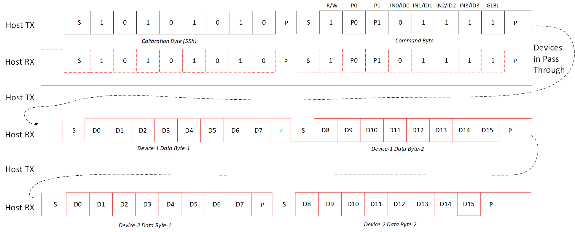
A global read command is indicated by C[0] = 1. As shown in Figure 7-13, the TMP144 with the device ID of 0000 then breaks the bus connection, transmits the data from the register indicated by bits C[2:1] (corresponding to data register pointer P[1:0]), and then reconnects the bus. The TMP144 with the device ID of 0001 then repeats the same sequence, followed by the rest of the TMP144 devices in the daisy-chain.

GUID-20200826-CA0I-78T9-1SLT-3SM4JV82SPFW-low.gif Figure 7-13 Global Read Command Flow.

Table 7-3 Pointer Addresses
P1 P0 REGISTER
0 0 Temperature register (read-only)
0 1 Configuration register (read/write)
1 0 TLOW register (read/write)
1 1 THIGH register (read/write)