SLUSBX9I March 2014 – July 2019 TPS23861
PRODUCTION DATA.
- 1 Features
- 2 Applications
- 3 Description
- 4 Revision History
- 5 Pin Configuration and Functions
- 6 Specifications
-
7 Detailed Description
- 7.1 Overview
- 7.2 Functional Block Diagram
- 7.3
Feature Description
- 7.3.1 Detection Resistance Measurement
- 7.3.2 Physical Layer Classification
- 7.3.3 Class and Detect Fields
- 7.3.4 Register State Following a Fault
- 7.3.5 Disconnect
- 7.3.6 Disconnect Threshold
- 7.3.7 Fast Shutdown Mode
- 7.3.8 Legacy Device Detection
- 7.3.9 VPWR Undervoltage and UVLO Events
- 7.3.10 Timer-Deferrable Interrupt Support
- 7.3.11 A/D Converter and I2C Interface
- 7.3.12 Independent Operation when the AUTO Bit is Set
- 7.3.13 I2C Slave Address and AUTO Bit Programming
- 7.4 Device Functional Modes
- 7.5
Register Map – I2C-Addressable
- 7.5.1 Interrupt Register
- 7.5.2 Interrupt Enable Register
- 7.5.3 Power Event Register
- 7.5.4 Detection Event Register
- 7.5.5 Fault Event Register
- 7.5.6 Start/ILIM Event Register
- 7.5.7 Supply Event Register
- 7.5.8 Port n Status Register
- 7.5.9 Power Status Register
- 7.5.10 I2C Slave Address Register
- 7.5.11 Operating Mode Register
- 7.5.12 Disconnect Enable Register
- 7.5.13 Detect/Class Enable Register
- 7.5.14 Port Power Priority Register
- 7.5.15 Timing Configuration Register
- 7.5.16 General Mask 1 Register
- 7.5.17 Detect/Class Restart Register
- 7.5.18 Power Enable Register
- 7.5.19 Reset Register
- 7.5.20 Legacy Detect Mode Register
- 7.5.21 Two-Event Classification Register
- 7.5.22 Interrupt Timer Register
- 7.5.23 Disconnect Threshold Register
- 7.5.24 ICUTnm CONFIG Register
- 7.5.25 Temperature Register
- 7.5.26 Input Voltage Register
- 7.5.27 Port n Current Register
- 7.5.28 Port n Voltage Register
- 7.5.29 PoE Plus Register
- 7.5.30 Firmware Revision Register
- 7.5.31 I2C Watchdog Register
- 7.5.32 Device ID Register
- 7.5.33 Cool Down/Gate Drive Register
- 7.5.34 Port n Detect Resistance Register
- 7.5.35 Port n Detect Voltage Difference Register
- 7.5.36 Reserved Registers
-
8 Application and Implementation
- 8.1 Introduction to PoE
- 8.2 Application Information
- 8.3 Typical Application
- 8.4 System Examples
- 9 Power Supply Recommendations
- 10Layout
- 11Device and Documentation Support
- 12Mechanical, Packaging, and Orderable Information
Package Options
Mechanical Data (Package|Pins)
- PW|28
Thermal pad, mechanical data (Package|Pins)
- PW|28
Orderable Information
7.3.11 A/D Converter and I2C Interface
The TPS23861 features five multi-slope integrating converters. Each of the first four converters is dedicated to current measurement for one port and is operated independently to perform measurements. The converters are used for current monitoring (100 ms averaged) and disconnect. The fifth converter is shared between all four ports for detection (conversion time set by MAINS bit), port voltage monitoring, Power Good Status and FET short detection (1 ms for all). It is also used for general-purpose measurements including input voltage (1 ms) and temperature.
The A/D converter type used in the TPS23861 differs from other types of converters in that it converts while the input signal is being sampled by the integrator, resulting in reduced conversion time and providing inherent filtering over the conversion period. The typical conversion time of the current converters is 800 µs. Digital averaging is used to provide a port current measurement integrated over a 100-ms time period.
NOTE
An anti-aliasing filter is present for current and voltage monitoring. Port current conversions are performed continuously.
Powered device (PD) detection is performed by averaging 16 consecutive samples providing significant rejection of noise at 50/60-Hz line frequency. The total time for the 16 samples can be set to 20 ms or 16.7 ms by the MAINS bit to correspond to the local mains frequency.
The fifth converter continuously measures drain voltages from one port to the next one, updating internal registers used for Power Good Status and FET short detection, unless a command is received to perform a specific measurement.
Also, when the port is powered on, the tSTART timer (used during PD power-on inrush) must expire before any current or voltage A/D conversion can begin for the first four converters.
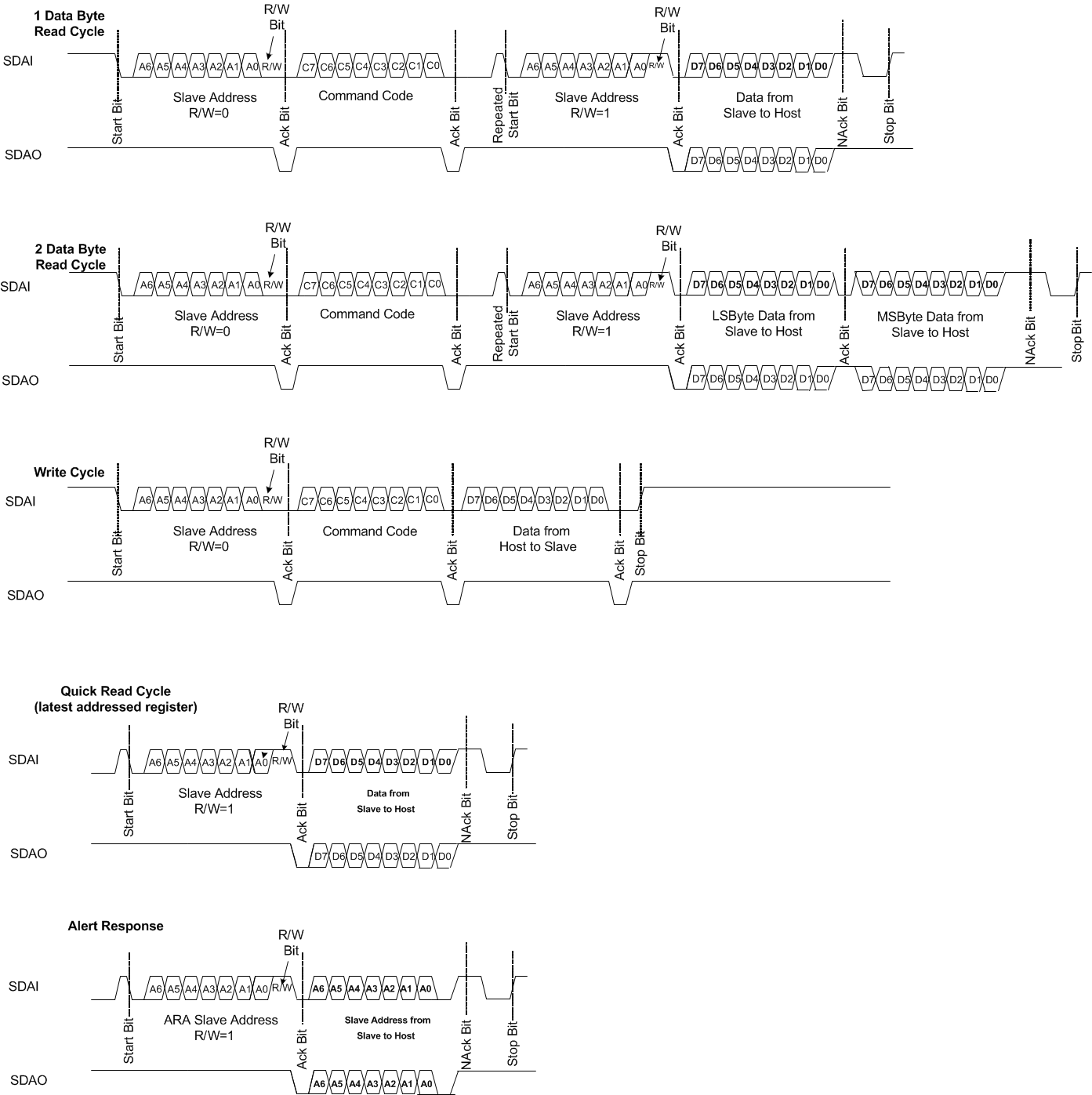
Figure 40 illustrates read and write operations through I2C interface. The two-data-bytes-read operation is applicable to A/D conversion results.
It is also possible to perform an I2C write operation to many TPS23861 devices at same time. The slave address during this broadcast access is 0x30.
The TPS23861, using the INT pin, supports the SMBALERT protocol. When INT is asserted low, if the bus master controller sends the alert response address, the TPS23861 responds providing its device address on the SDA line and releases the INT line. If there is a collision between two TPS23861 devices responding simultaneously, then the device with the lower address wins arbitration and responds first, by use of SDAI and SDAO lines.
An I2C watchdog timer is also available on the TPS23861, which monitors the I2C clock line in order to prevent hung software situations that could leave ports in a hazardous state. The timer can be reset by either edge on the SCL line. When enabled, if the watchdog timer expires, all ports are turned off and WDS bit is set. The nominal watchdog time-out period is 2 seconds. See I2C Watchdog Register for more details on the subject.
NOTE
When a stop condition is detected on the I2C bus after having at least received the command byte, the TPS23861 stores the command byte in an internal register.
NOTE
When using the I2C interface the host software should wait 22 ms minimum after a reset to ensure valid I2C transactions.
This content can be later used as a register address pointer during next quick read cycle register access. See Figure 40. This internal register is cleared at power on or through the RESET pin.
 Figure 40. I2C/SMBus Interface Read and Write Protocol