SNVSAU8A June 2017 – February 2024 TPS549B22
PRODUCTION DATA
- 1
- 1 Features
- 2 Applications
- 3 Description
- 4 Pin Configuration and Functions
- 5 Specifications
-
6 Detailed Description
- 6.1 Overview
- 6.2 Functional Block Diagram
- 6.3 Feature Description
- 6.4 Device Functional Modes
- 6.5 Programming
-
7 Register Maps
- 7.1 OPERATION Register (address = 1h)
- 7.2 ON_OFF_CONFIG Register (address = 2h)
- 7.3 CLEAR FAULTS (address = 3h)
- 7.4 WRITE PROTECT (address = 10h)
- 7.5 STORE_DEFAULT_ALL (address = 11h)
- 7.6 RESTORE_DEFAULT_ALL (address = 12h)
- 7.7 CAPABILITY (address = 19h)
- 7.8 VOUT_MODE (address = 20h)
- 7.9 VOUT_COMMAND (address = 21h)
- 7.10 VOUT_MARGIN_HIGH (address = 25h) ®
- 7.11 VOUT_MARGIN_LOW (address = 26h)
- 7.12 STATUS_BYTE (address = 78h)
- 7.13 STATUS_WORD (High Byte) (address = 79h)
- 7.14 STATUS_VOUT (address = 7Ah)
- 7.15 STATUS_IOUT (address = 7Bh)
- 7.16 STATUS_CML (address = 7Eh)
- 7.17 MFR_SPECIFIC_00 (address = D0h)
- 7.18 MFR_SPECIFIC_01 (address = D1h)
- 7.19 MFR_SPECIFIC_02 (address = D2h)
- 7.20 MFR_SPECIFIC_03 (address = D3h)
- 7.21 MFR_SPECIFIC_04 (address = D4h)
- 7.22 MFR_SPECIFIC_06 (address = D6h)
- 7.23 MFR_SPECIFIC_07 (address = D7h)
- 7.24 MFR_SPECIFIC_44 (address = FCh)
-
8 Application and Implementation
- 8.1 Application Information
- 8.2
Typical Applications
- 8.2.1 TPS549B22 1.5-V to 18-V Input, 1-V Output, 25-A Converter
- 8.2.2 Design Requirements
- 8.2.3
Detailed Design Procedure
- 8.2.3.1 Custom Design With WEBENCH® Tools
- 8.2.3.2 Switching Frequency Selection
- 8.2.3.3 Inductor Selection
- 8.2.3.4 Output Capacitor Selection
- 8.2.3.5 Input Capacitor Selection
- 8.2.3.6 Bootstrap Capacitor Selection
- 8.2.3.7 BP Pin
- 8.2.3.8 R-C Snubber and VIN Pin High-Frequency Bypass
- 8.2.3.9 Optimize Reference Voltage (VSEL)
- 8.2.3.10 MODE Pin Selection
- 8.2.3.11 ADDR Pin Selection
- 8.2.3.12 Overcurrent Limit Design
- 8.2.4 Application Curves
- 8.3 Power Supply Recommendations
- 8.4 Layout
- 9 Device and Documentation Support
- 10Revision History
- 11Mechanical, Packaging, and Orderable Information
Package Options
Refer to the PDF data sheet for device specific package drawings
Mechanical Data (Package|Pins)
- RVF|40
Thermal pad, mechanical data (Package|Pins)
- RVF|40
Orderable Information
8.2.3.12 Overcurrent Limit Design
The TPS549B22 device uses the ILIM pin to set the OCP level. Connect the ILIM pin to GND through the voltage setting resistor, RILIM. To provide both good accuracy and cost effective solution, this device supports temperature compensated MOSFET on-resistance (RDS(on)) sensing. Also, this device performs both positive and negative inductor current limiting with the same magnitudes. Positive current limit is normally used to protect the inductor from saturation therefore causing damage to the high-side and low-side FETs. Negative current limit is used to protect the low-side FET during OVP discharge.
The inductor current is monitored by the voltage between PGND pin and SW pin during the OFF time. The ILIM pin has 1200 ppm/°C temperature slope to compensate the temperature dependency of the on-resistance. The PGND pin is used as the positive current sensing node.
TPS549B22 has cycle-by-cycle over-current limiting control. The inductor current is monitored during the OFF state and the controller maintains the OFF state during the period that the inductor current is larger than the overcurrent ILIM level. The voltage on the ILIM pin (VILIM) sets the valley level of the inductor current. The range of value of the RILIM resistor is between 9.53 kΩ and 105 kΩ. The range of valley OCL is between 5 A and 50 A (typical). If the RILIM resistance is outside of the recommended range, OCL accuracy and function cannot be ensured. (see Table 8-3)
| 1% RILIM (kΩ) | OVERCURRENT PROTECTION VALLEY (A) |
| 82.1 | 40 |
| 71.5 | 35 |
| 61.9 | 30 |
| 51.1 | 25 |
| 40.2 | 20 |
| 30.1 | 15 |
| 20.5 | 10 |
Use Equation 15 to relate the valley OCL to the RILIM resistance.
where
- RILIM is in kΩ
- OCLVALLEY is in A
In this design example, the desired valley OCL is 43 A, the calculated RILIM is 61.9 kΩ. Use Equation 16 to calculate the DC OCL to be 32.1 A.

where
- RILIM is in kΩ
- OCLDC is in A
In an overcurrent condition, the current to the load exceeds the inductor current and the output voltage falls. When the output voltage crosses the under-voltage fault threshold for at least 1 ms, the behavior of the device depends on the VSEL pin strap setting. If hiccup mode is selected, the device restarts after a 16-ms delay (1-ms soft-start option). If the overcurrent condition persists, the OC hiccup behavior repeats. During latch-off mode operation the device shuts down until the EN pin is toggled or VDD pin is power cycled.

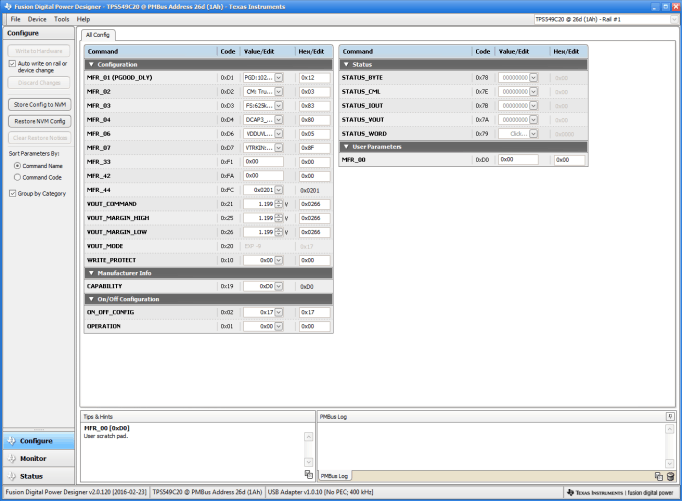
 Figure 8-2 VOUT Command Graphic User Interface