SLUSD37E October 2017 – November 2019 UCC28056
PRODUCTION DATA.
- 1 Features
- 2 Applications
- 3 Description
- 4 Revision History
- 5 Device Comparison Tables
- 6 Pin Configuration and Functions
- 7 Specifications
-
8 Detailed Description
- 8.1 Overview
- 8.2 Functional Block Diagram
- 8.3
Feature Description
- 8.3.1 CrM/DCM Control Principle
- 8.3.2 Line Voltage Feed-Forward
- 8.3.3 Valley Switching and CrM/DCM Hysteresis
- 8.3.4 Transconductance Amplifier with Transient Speed-up Function
- 8.3.5 Faults and Protections
- 8.3.6 High-Current Driver
- 8.4 Controller Functional Modes
- 9 Application and Implementation
- 10Power Supply Recommendations
- 11Layout
- 12Device and Documentation Support
- 13Mechanical, Packaging, and Orderable Information
Package Options
Mechanical Data (Package|Pins)
- DBV|6
Thermal pad, mechanical data (Package|Pins)
Orderable Information
9.2.2.2.1 Boost Inductor Design
The minimum equivalent resistance presented, to the Line, by the input of the Boost PFC stage changes according to the current Line Feed-Forward setting. RInEqMin0 and RInEqMin1 present the minimum equivalent input resistance for the first two Line Feed-Forward levels.


Equation 15 calculates the maximum input power that can be drawn from a given Line voltage. The maximum input power is set to 110% of POutMax to account for power stage efficiency.

Equation 16 calculates the Boost inductance value required to ensure that maximum load can be delivered from minimum Line voltage.

Ensure that POutMax can be delivered from the lowest Line voltage for GFF1. Use Equation 17 to calculate the required Boost inductor value .

Choose the lower of the two values calculated in Equation 16 and Equation 17 (LBST0 and LBST1). Using a smaller inductance value compromises light load efficiency. A larger inductance value cannot deliver the required maximum load power (POutMax) across the required range of Line voltage.
Choose a Boost inductor value of 200 µH, considering a tolerance of 10%. In order to deliver maximum load power the inductor must be able to operate with a peak current that is greater than both ILPk0 and ILPk1


Use Equation 22 to calculate a current sense resistance that ensures the required peak inductor current (ILPk) does not cause early termination of the TON period.

Achieve this amount of resistance by connecting three resistors in parallel.

Use Equation 24 to calculate an inductance value that allows a saturation current above the maximum Ocp1 current limit value.

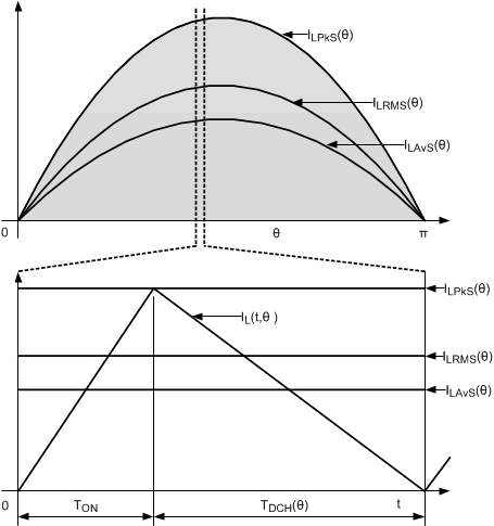
Maximum current in the power components flows while delivering maximum load when supplied from minimum Line voltage. In this condition, the UCC28056 controller always operates in transition mode (CrM). shows the inductor current waveforms for ideal CrM operation.
 Figure 27. Ideal Transition Mode (CrM) Inductor Current
 Equation 25 describes the he Boost inductor RMS current over a single switching cycle, at angle θ through the Line half-cycle.

Equation 26 describes the Boost inductor RMS current over a complete Line cycle.

Maximum Boost inductor RMS current occurs at minimum Line voltage and maximum input power.

Based upon the inductor requirements, a custom magnetic can be designed, or a suitable catalogue controller selected.
Table 2. Inductor Requirements
| Description | Value | Unit |
|---|---|---|
| Inductance | 200 | µH |
| RMS Current | 2.5 | A |
| Saturation Current | 8.8 | A |