SLUSD37E October 2017 – November 2019 UCC28056
PRODUCTION DATA.
- 1 Features
- 2 Applications
- 3 Description
- 4 Revision History
- 5 Device Comparison Tables
- 6 Pin Configuration and Functions
- 7 Specifications
-
8 Detailed Description
- 8.1 Overview
- 8.2 Functional Block Diagram
- 8.3
Feature Description
- 8.3.1 CrM/DCM Control Principle
- 8.3.2 Line Voltage Feed-Forward
- 8.3.3 Valley Switching and CrM/DCM Hysteresis
- 8.3.4 Transconductance Amplifier with Transient Speed-up Function
- 8.3.5 Faults and Protections
- 8.3.6 High-Current Driver
- 8.4 Controller Functional Modes
- 9 Application and Implementation
- 10Power Supply Recommendations
- 11Layout
- 12Device and Documentation Support
- 13Mechanical, Packaging, and Orderable Information
Package Options
Mechanical Data (Package|Pins)
- DBV|6
Thermal pad, mechanical data (Package|Pins)
Orderable Information
9.2.2.5.2 Compensator Design
The integrator response of the plant provides a gain roll off of –20dB/decade and introduces a phase lag of 90°. A simple integrating compensation network provides unacceptable phase margin because it introduces a second 90° of phase lag into the voltage loop. To ensure adequate phase margin, use a type 2 compensation network to provide the desired phase boost a the gain cross-over frequency. Equation 84 describes the mall-signal gain of the error amplifier and type 2 compensation network.

may also be expressed as follows:

where


Rearranging Equation 86, Equation 87 and Equation 88 yields:


For maximum phase Boost at the gain cross-over frequency, compensator design proceeds by placing the pole and zero an equal distance above and below the gain cross-over frequency (fB) on the Bode plot. Because the frequency axis is logarithmic this yields the following pole (fP) and zero (fZ) frequencies:


Phase margin of the loop is equal to the phase boost provided by the type 2 compensator, because the underlying integrator characteristics of the plant and compensator combine to provide 180° of phase lag. To achieve the desired phase margin (ΦPM) at fB the separation between the pole and zero frequencies may be found by substituting Equation 92 and Equation 93 into Equation 85, and solving for K in terms of the phase boost angle.

The next step is to select the desired phase margin. A typical phase margin range 45° to 75°. For this example design a target phase margin of 65° is selected.


The next step is to determine the loop gain cross-over frequency (fB). A faster loop, results in more twice Line frequency ripple on the COMP pin voltage, leading to increased Line current distortion.
Begin by setting a target of 1% third harmonic distortion due to twice Line frequency COMP voltage ripple. To achieve this target, the twice Line frequency COMP pin ripple must be less than 2% of the DC value during steady-state full power operation. The design proceeds by selecting the loop gain cross-over frequency (fB) that ensures twice Line frequency COMP pin ripple amplitude does not exceed 2% of its DC level.
Use Equation 97 to calculate twice Line frequency voltage ripple amplitude across the output capacitor.

The output voltage ripple amplitude must be attenuated by the feedback network to meet our target of 2% ripple amplitude on the COMP pin voltage.

Equation 99 simplifies Equation 98.

where
- 2 x fLine >> fP
- 2 x fLine >> fZ
Equation 100 describes unity at the gain cross-over frequency.

Equation 100 can also be expressed as shown in Equation 101.

Calculate the pole and zero frequencies using Equation 92 and Equation 93. Then determine the compensation component values using Equation 89, Equation 90 and Equation 91.


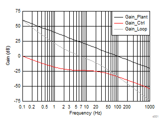
 Figure 31. Gain vs Frequency
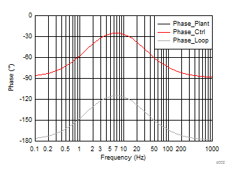
  Figure 32. Phase vs Frequency