SLUSD37E October 2017 – November 2019 UCC28056
PRODUCTION DATA.
- 1 Features
- 2 Applications
- 3 Description
- 4 Revision History
- 5 Device Comparison Tables
- 6 Pin Configuration and Functions
- 7 Specifications
-
8 Detailed Description
- 8.1 Overview
- 8.2 Functional Block Diagram
- 8.3
Feature Description
- 8.3.1 CrM/DCM Control Principle
- 8.3.2 Line Voltage Feed-Forward
- 8.3.3 Valley Switching and CrM/DCM Hysteresis
- 8.3.4 Transconductance Amplifier with Transient Speed-up Function
- 8.3.5 Faults and Protections
- 8.3.6 High-Current Driver
- 8.4 Controller Functional Modes
- 9 Application and Implementation
- 10Power Supply Recommendations
- 11Layout
- 12Device and Documentation Support
- 13Mechanical, Packaging, and Orderable Information
Package Options
Mechanical Data (Package|Pins)
- DBV|6
Thermal pad, mechanical data (Package|Pins)
Orderable Information
9.2.2.3 ZCD/CS Pin
An external divider network attached to the ZCD/CS pin transfers both the attenuated Drain voltage waveform (VDS) and the current sense signal (VCS) into the controller. This transfer is possible because the current sense signal requires observation only when the switch is ON and the VDS signal is close to zero. While the Drain voltage waveform requires sensing only when the switch is OFF and the current sense signal is close to zero.

Equation 52 describes the attenuated Drain voltage during the on-time period when the MOSFET is switched ON.

The ON state resistance of the MOSFET (RDSON) typically has a similar value to the current sense resistor (RCS). The attenuation of the divider (ZZC1, ZZC2) is 1/401 and hence the second term of Equation 52 may be neglected.

Hence the required current sense resistor value can be calculated from the maximum peak inductor current obtained in
Outside the TON period, when the MOSFET is switched OFF, the current flowing through the current sense resistor is close to zero. In this case Equation 51 may be expressed as follows.

UCC28056 prevents the start of a new switching cycle until increasing negative slope is detected on the ZCD/CS pin voltage waveform. The increasing negative slope indicates that the inductor current has fallen to zero so the output diode is already OFF. Turn-ON switching loss is further reduced by synchronizing the start of each new switching cycle with a minimum, or valley, on the Drain waveform.
In theory, a simple resistor divider can be used to attenuate the Drain voltage waveform fed into the ZCD/CS pin. In practice, the parasitic capacitance associated with the PCB traces and the ZCD/CS pin filter the attenuated signal and introduce phase shift. The resulting distortion and phase shift negatively impact the ability of the part to synchronize to the zero inductor current transitions. The problem is compounded by the need to limit power dissipation in the resistive divider, which dictates the use of high resistance values, and increased filtering of the attenuated signal.
Add a capacitor divider in parallel with the resistor divider in order to use of high value resistors without introducing filtering and associated phase shift. In this case, ensure that the reactive divider ratio is equal to the resistor divider ratio.

Hence:

There are number of internal voltage thresholds driven by the attenuated Drain voltage signal supplied to the ZCD/CS pin. These include Brown-Out (VZCBoRise), Line feed-forward (VFFxRise, VFFxFall) and second output over-voltage (VOvp2Th). The same external divider ratio (KZC) drives all of these thresholds. Scope to vary the attenuation ratio specified is limited because it impacts all of these thresholds in unison.


The controller infers Line voltage from the switching cycle average voltage on the Drain node. Neglecting any resistive voltage drop in the Boost inductor this must be equal to the voltage supplied from the input rectifier, provided the Boost inductor current returns to zero at the end of each cycle (TM/CrM/DCM). Voltage drops in the input rectifier bridge and EMI filter stage cause an error between predicted and measured threshold values. An internal peak detector determines the peak input voltage across a Line half-cycle. Equation 58 above converts this peak value to an RMS quantity, but assumes an ideal sinusoidal Line supply
Equation 59 calculates the output voltage required to trigger the second output overvoltage comparator (Ovp2).

This parameter is observed via the Drain waveform, voltage drops in the Boost Diode and series NTC resistor, causes the Ovp2 comparator to trip at a lower output voltage level.
Power dissipation in the Drain sensing resistor divider chain reaches its highest value during the Burst OFF condition. During the Burst OFF condition, the Drain voltage approximates a DC voltage equal to the Line voltage peak. This approximation assumes the time constant CIN × (RZC1+ RZC2) is long compared with a Line half-period. Under no-load conditions, the Burst OFF duty cycle is high therefore maximum power dissipation in the Drain sensing resistor divider chain, occurs at high Line and no-load, as described in Equation 60.

Equation 61 calculates the maximum value of RZC1 c, allowing a budget of 1% error due to input bias current (IZCBias), on the lowest voltage threshold (VZCBoRise).

The upper resistor in the divider chain (RZC1) must withstand the peak output voltage under a surge test. For a rugged solution, the resistor(s) in this location must have a voltage rating above the avalanche rating of the Boost MOSFET. This design uses a series chain of three 1206, SMT, 3.24 MΩ resistors for this location, which yields DC voltage withstand capability above 600 V.


Use Equation 60 to calculate the power dissipation in the ZCD/CS pin divider resistors.

Once arranged on the PCB, the resistor divider circuit has some parasitic capacitance across both the upper (RZC1) and lower (RZC2) resistors. Experience suggests a parasitic capacitance (CZC1) of approximately 0.1 pF across resistor RZC1, when it is made up of three 1206 SMT components, assuming a compact PCB layout. In theory this parasitic capacitance could be used to form the entire value of CZC1 and an appropriate value of CZC2 added to achieve the ratio required by Equation 56. In practice most designers choose to add an explicit capacitor in this location to improve tolerance to small changes in layout, such as may occur when connecting oscilloscope probes. Ensure the time constant for the divider does not extend over many switching cycles. This limitation ensures that Line surge or system ESD transient events may disturb the ZCD/CS pin DC level but does not persist over an excessive number of switching cycles.
Select a single 10-pF, 1000-V, 0805 SMT capacitor with 5% tolerance.

Use Equation 66 calculate the lower divider capacitor value.

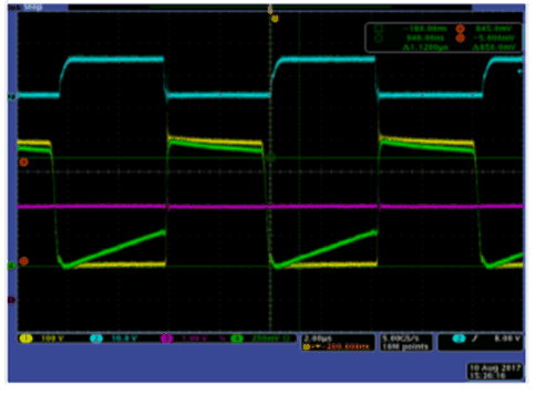
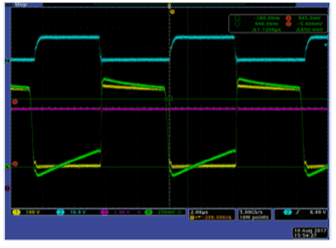
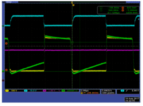
In practice, once the final PCB layout is complete, adjust the lower capacitor value to account for parasitic capacitances present on the PCB. Consider both the Drain and ZCD/CS pin waveforms and adjust the lower capacitance value (CZC2) until the value allows the required ratio in signal amplitude. Use a low capacitance probe for the ZCD/CS pin connection. Figure 28, Figure 29 and Figure 30 present the type of waveforms that occur during this tuning process.

| CH1 = VDS | CH2 = VDR |
| CH3 = VCO | CH3 = VZC |

| CH1 = VDS | CH2 = VDR | ||
| CH3 = VCO | CH3 = VZC |

| CH1 = VDS | CH2 = VDR |
| CH3 = VCO | CH3 = VZC |