JAJSBK7H January 2012 – February 2018 DS125DF410
PRODUCTION DATA.
- 1 特長
- 2 アプリケーション
- 3 概要
- 4 改訂履歴
- 5 Pin Configuration and Functions
- 6 Specifications
-
7 Detailed Description
- 7.1 Overview
- 7.2 Functional Block Diagram
- 7.3 Feature Description
- 7.4 Device Functional Modes
- 7.5
Programming
- 7.5.1 SMBus Strap Observation
- 7.5.2 Device Revision and Device ID
- 7.5.3 Control/Shared Register Reset
- 7.5.4 Interrupt Channel Flag Bits
- 7.5.5 SMBus Master Mode Control Bits
- 7.5.6 Resetting Individual Channels of the Retimer
- 7.5.7 Interrupt Status
- 7.5.8 Overriding the CTLE Boost Setting
- 7.5.9 Overriding the VCO Search Values
- 7.5.10 Overriding the Output Multiplexer
- 7.5.11 Overriding the VCO Divider Selection
- 7.5.12 Using the PRBS Generator
- 7.5.13 Using the Internal Eye Opening Monitor
- 7.5.14 Overriding the DFE Tap Weights and Polarities
- 7.5.15 Enabling Slow Rise/Fall Time on the Output Driver
- 7.5.16 Inverting the Output Polarity
- 7.5.17 Overriding the Figure of Merit for Adaptation
- 7.5.18 Setting the Rate and Subrate for Lock Acquisition
- 7.5.19 Setting the Adaptation/Lock Mode
- 7.5.20 Initiating Adaptation
- 7.5.21 Setting the Reference Enable Mode
- 7.5.22 Overriding the CTLE Settings Used for CTLE Adaptation
- 7.5.23 Setting the Output Differential Voltage
- 7.5.24 Setting the Output De-Emphasis Setting
- 7.6 Register Maps
- 8 Application and Implementation
- 9 Power Supply Recommendations
- 10Layout
- 11デバイスおよびドキュメントのサポート
- 12メカニカル、パッケージ、および注文情報
パッケージ・オプション
メカニカル・データ(パッケージ|ピン)
- RHS|48
サーマルパッド・メカニカル・データ
- RHS|48
発注情報
7.4.1 SMBus Master Mode and SMBus Slave Mode
In SMBus master mode the DS125DF410 reads its initial configuration from an external EEPROM upon power-up. A description of the operation of this mode appears in a separate application note.
Some of the pins of the DS125DF410 perform the same functions in SMBus master and SMBus slave mode. Once the DS125DF410 has finished reading its initial configuration from the external EEPROM in SMBus master mode it reverts to SMBus slave mode and can be further configured by an external controller over the SMBus. There are two pins that provide unique functions in SMBus master mode. These are as follows:
- ALL_DONE
- READ_EN
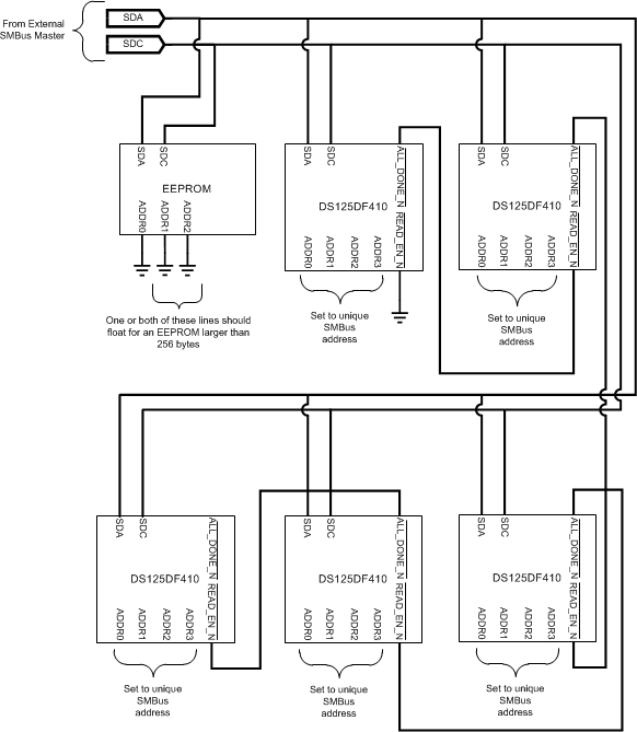
These pins are meant to work together. When the DS125DF410 is powered up in SMBus master mode, it reads its configuration from the external EEPROM when the READ_EN pin goes low. When the DS125DF410 is finished reading its configuration from the external EEPROM, it drives its ALL_DONE pin low. In applications where there is more than one DS125DF410 on the same SMBus, bus contention can result if more than one DS125DF410 tries to take command of the SMBus at the same time. The READ_EN and ALL_DONE pins prevent this bus contention.
The system should be designed so that the READ_EN pin of one of the DS125DF410s in the system is driven low on power-up. This DS125DF410 will take command of the SMBus on power-up and will read its initial configuration from the external EEPROM. When it is finished reading its configuration, it will set its ALL_DONE pin low. This pin should be connected to the READ_EN pin of another DS125DF410. When this DS125DF410 senses its READ_EN pin driven low, it will take command of the SMBus and read its initial configuration from the external EEPROM, after which it will set its ALL_DONE pin low. By connecting the ALL_DONE pin of each DS125DF410 to the READ_EN pin of the next DS125DF410, each DS125DF410 can read its initial configuration from the EEPROM without causing bus contention.
For SMBus slave mode, the READ_EN pin must be tied low. Do not leave it floating or tie it high.
A connection diagram showing several DS125DF410s along with an external EEPROM and an external SMBus master is shown in Figure 5 below. The SMBus master must be prevented from trying to take control of the SMBus until the DS125DF410s have finished reading their initial configurations from the EEPROM.
 Figure 5. Connection Diagram for Multiple DS125DF410s in SMBus Master Mode
In SMBus master mode after the DS125DF410 has finished reading its initial configuration from the external EEPROM it reverts to SMBus slave mode. In either mode the SMBus data and clock lines, SDA and SDC, are used. Also, in either mode, the SMBus address is latched in on the address strap lines on power-up. In SMBus slave mode, if the READ_EN pin is not tied low, the DS125DF410 will not latch in the address on its address strap lines. It will instead latch in an SMBus write address of 0x30 regardless of the state of the address strap lines. This is a test feature. Obviously a system with multiple retimers cannot operate properly if all the retimers are responding to the same SMBus address. Tie the READ_EN pin low when operating in SMBus slave mode to avoid this condition.
The DS125DF410 reads its SMBus address upon power-up from the SMBus address lines.