JAJU732C June 2019 – July 2022
- 概要
- Resources
- 特長
- アプリケーション
- 5
- 1System Description
- 2System Overview
- 3Circuit Description
- 4Hardware, Software, Testing Requirements, and Test Results
- 5Design Files
- 6Related Documentation
- 7Terminology
- 8About the Author
- 9Revision History
4.5.1 Open-Loop Performance
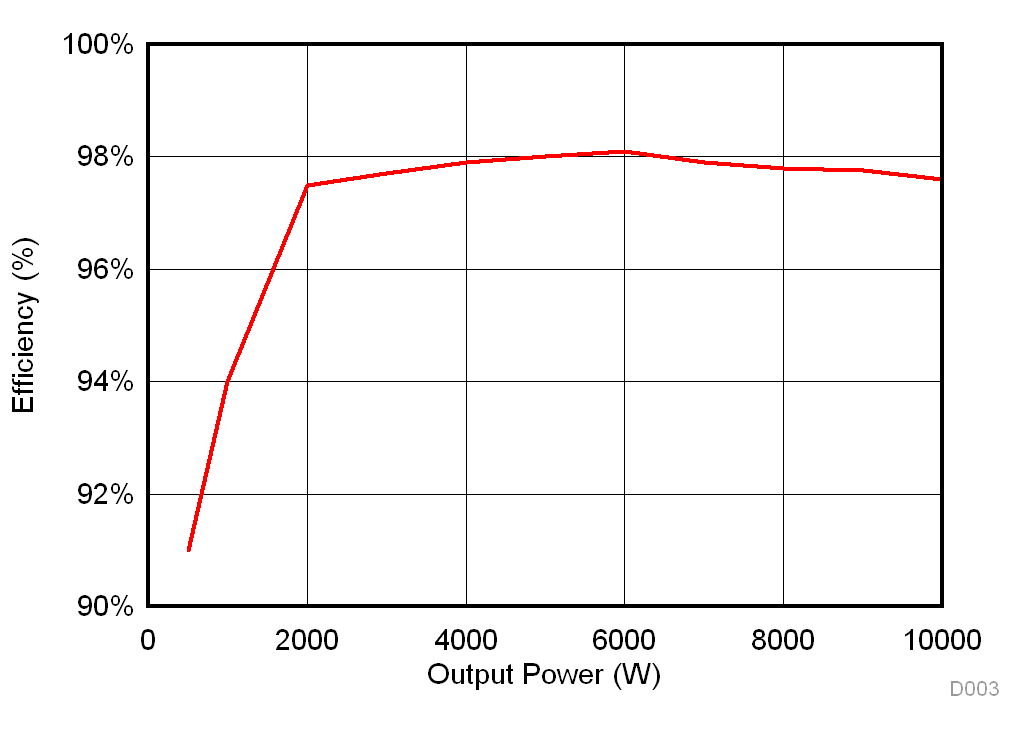
Table 4-4 shows the system efficiency as a function of output power. The converter output power was varied by changing the load and the phase angle between the input and output bridge to reach 10 kW. The table shows that the converter achieves a peak efficiency of 98.2% at approximately 6 kW and has a full load efficiency of 97.6% at 10 kW. Figure 4-45 shows the measured efficiency of the converter at different power levels.
| TESTING CONDITIONS | INPUT VOLTAGE VIN: 800 V, Switching frequency: 100 kHz, Phase shift: Between 10° to 15°, Load resistance: Decreased from 128 Ω to 34 Ω | INPUT VOLTAGE VIN: 800 V, Switching frequency: 100 kHz, Load resistance: 26 Ω, Phase shift: Increased from 16° to 23° | |||||||||
|---|---|---|---|---|---|---|---|---|---|---|---|
| Load in Watts | 500 | 1000 | 2000 | 3000 | 4000 | 5000 | 6000 | 7000 | 8000 | 9000 | 10000 |
| Efficiency | 91% | 94% | 97.50% | 97.70% | 97.90% | 98% | 98.16% | 97.90% | 97.80% | 97.75% | 97.60% |
 Figure 4-45 Efficiency Versus Output Power
Table 4-5 shows the resistive loads that were used to vary the output power from light load to full load. The input voltage is kept constant at 800 V. As seen from the table, to achieve power transfer of 10 kW, the phase angle is varied by keeping the load resistance fixed at 26 Ω. For a particular power output, input voltage, output voltage, switching frequency, turns ratio, and leakage inductance, the phase angle is calculated using Equation 14.
| INPUT CURRENT (A) | INPUT POWER (W) | OUTPUT CURRENT (A) | OUTPUT VOLTAGE (V) | OUTPUT POWER (W) | EFFICIENCY | LOAD RESISTANCE (Ω) | OBSERVED PHASE SHIFT (deg) | ACTUAL CALCULATED PHASE SHIFT (deg) |
|---|---|---|---|---|---|---|---|---|
| 2.47 | 1976 | 3.875 | 496 | 1922 | 97.3% | 128 | 10 | 7 |
| 4.37 | 3496 | 7.07 | 483.4 | 3416 | 97.7% | 68 | 10 | 7 |
| 5.51 | 4408 | 9.06 | 473 | 4286 | 97.2% | 52 | 10 | 8.5 |
| 7.79 | 6232 | 13.42 | 455.6 | 6114 | 98.1% | 34 | 15 | 13 |
| 8.86 | 7088 | 16.49 | 419.4 | 6916 | 97.6% | 26 | 16.2 | 16.32 |
| 11.56 | 9248 | 18.85 | 479.4 | 9036 | 97.7% | 26 | 21.6 | 18.9 |
| 12.62 | 10096 | 19.68 | 500.5 | 9855 | 97.6% | 26 | 23 | 20 |
Table 4-5 shows that the observed phase shift (calculated from the PWM settings) and the actual phase shift calculated from formula varies slightly. The theoretical formula gives a good starting point to set the phase shift, but depending on the load applied to the converter, there is a requirement for fine adjustment of phase to deliver the required power. At a phase shift of 23 degrees, full power transfer of 10 kW and an output voltage of 500 V for an input voltage of 800 V at a switching frequency of 100 kHz are obtained. The closed-loop regulation of output voltage to the desired value by controlling phase is being implemented and will be available following the release of this design.
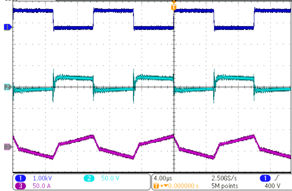
Figure 4-46 shows the drain voltage (dark blue), gate voltage (cyan), and inductor current (purple) waveforms of the primary side SiC MOSFET at a 10-kW power level. The drain voltage switches between zero and 800 V, the gate voltage waveform switches from +15 / –4 V, and the inductor current has a trapezoidal signature with peak current of approximately 20 A.
 Figure 4-46 Waveforms at 10 kW
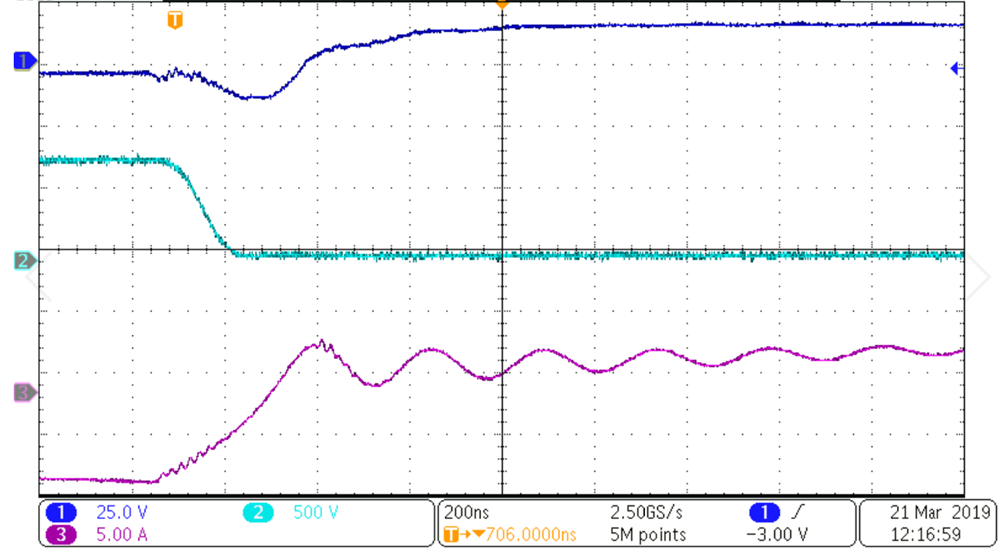
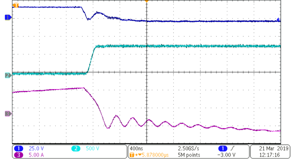
Figure 4-47 shows the waveforms at the instant of turn on. Gating pulses (dark blue) are applied to turn on the MOSFET once the drain voltage (cyan) falls to zero. This results in ZVS turn on of the MOSFET. Figure 4-48 shows the switch turn off waveform. The turn off process results in switching losses. This can be minimized by placing output capacitors across MOSFETs.
 Figure 4-47 Switch Turn on Waveforms
 Figure 4-48 Switch Turn Off Waveforms
Table 4-6 shows the dimensions of the converter. The calculated total power density of the converter is 2.32 kW/L, which is more than our targeted specification of 1 kW/L.
| AXIS | DIMENSIONS |
|---|---|
| X | 328 mm |
| Y | 160 mm |
| Z | 82 mm |
| Volume | 4.3 liter |