JAJU732C June 2019 – July 2022
- 概要
- Resources
- 特長
- アプリケーション
- 5
- 1System Description
- 2System Overview
- 3Circuit Description
- 4Hardware, Software, Testing Requirements, and Test Results
- 5Design Files
- 6Related Documentation
- 7Terminology
- 8About the Author
- 9Revision History
4.4.3 Lab 3
In the lab 3 build, the board is excited in secondary voltage close-loop ( DAB_vSecSensed_Volts).
This lab runs the voltage mode compensator, obtain open-loop transfer function of plant from SFRA, and design compensator for the plant in compensator design tool.
Launch the compensation designer which prompts to select a valid SFRA data file. Import the SFRA data from the run in lab 2 into the compensation designer to design a 2P2Zcompensator. Keep more margins during this iteration of the design to ensure that when the loop is closed, the system is stable. The following coefficient values are hard-coded in the SW. The compensation designer GUI gives information about the stability of the loop, gain margin, phase margin, and bandwidth of the loop. The coefficients can be modified in the compensation designer GUI.
#define DAB_GV_2P2Z_A1 ((float32_t) -1.8756666)
#define DAB_GV_2P2Z_A2 (float32_t) 0.8756666
#define DAB_GV_2P2Z_B0 (float32_t) 3.0092688
#define DAB_GV_2P2Z_B1 ((float32_t) -5.8788593)
#define DAB_GV_2P2Z_B2 (float32_t) 2.8696427- Test Setup for Lab 3 (Closed Voltage Loop -
Vsec)
Compile the project by selecting Lab 3: Closed Loop Voltage with Resistive Load in the drop-down menu of Project Options from PowerSUITE GUI. Ensure current and voltage limits are set per operating conditions.
#if DAB_LAB == 3
#define DAB_CONTROL_RUNNING_ON C28X_CORE
#define DAB_POWER_FLOW DAB_POWER_FLOW_PRIM_SEC
#define DAB_INCR_BUILD DAB_CLOSED_LOOP_BUILD
#define DAB_TEST_SETUP DAB_TEST_SETUP_RES_LOAD
#define DAB_PROTECTION DAB_PROTECTION_ENABLED
#define DAB_CONTROL_MODE DAB_VOLTAGE_MODE
#define DAB_SFRA_TYPE 2
#define DAB_SFRA_AMPLITUDE (float32_t)DAB_SFRA_INJECTION_AMPLITUDE_LEVEL2
#endif
Use the following steps to run voltage close loop:
- Run the project by clicking green run button in CCS
- Populate the required
variables in the watch window by loading javascript '
setupdebugenv_lab3.js' in the scripting console
 Figure 4-34 Lab 3 Watch
View Configuration
 - Enable PWM by writing “1” to the DAB_clearTrip variable
- In the watch view, check if the DAB_vPrimSensed_Volts,
DAB_iPrimSensed_Amps, DAB_vSecSensed_Volts, and DAB_iSecSensed_Amps
variables are updating periodically
 Figure 4-35 Lab 3 Watch
View - Enable Closed Loop
 - Set the output voltage by writing to DAB_vSecRef_Volts (in this example 200Vdc)
- Enable closed loop
operation by writing “1” to the DAB_closeGvLoop variable. The controller
automatically adjusts the phase shift from default 0.032 to 0.04178,
depending upon the operating conditions to generate secondary output
voltage to match with that of DAB_vSecRef_Volts. Note: In the software the maximum phase shift is limited to 0.065 as a safety precaution. Adjust the primary voltage to stay within the phase shift limits and still generate the required secondary voltage. Alternatively, the maximum allowed phase shift can be modified to 0.15 in the code.
- Slowly increase the input VPRIM DC voltage and adjust DAB_vSecRef_Volts accordingly to reach to the required operating point
- Test the closed-loop operation by varying DAB_vSecRef_Volts from 400 V to 500 V. Observe that the DAB_vSecSensed_Volts tracks this command reference.
- Frequency response of closed loop voltage
- Run the SFRA by clicking on the SFRA icon. The SFRA GUI opens.
- Select the options for the device on the SFRA GUI; for example, for F280049, select floating point. Click the Setup Connection button. In the pop-up window, uncheck the boot-on-connect option and select an appropriate COM port. Select the OK button. Return to the SFRA GUI and click the Connect button.
- The SFRA GUI connects to the device. An SFRA sweep can now be started by clicking the Start Sweep button. The complete SFRA sweep takes a few minutes to finish. Monitor the activity in the progress bar on the SFRA GUI or by checking the flashing blue LED on the back of the control card, which indicates UART activity.
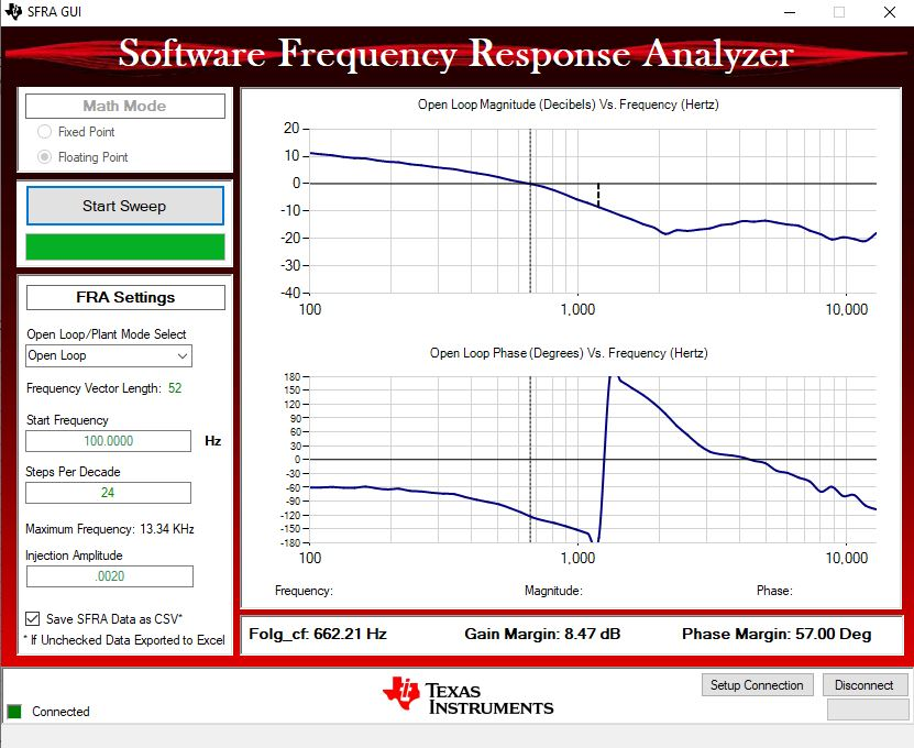
The bode plot in Figure 4-36 is captured using a DF22 compensator.
 Test condition: VIN = 600 V, IIN = 4.78 A, VOUT = 425 V, SFRA Amplitude = 0.002Figure 4-36 Lab 3 SFRA Open Loop Plot for the Closed Voltage Loop