JAJU732C June 2019 – July 2022
- 概要
- Resources
- 特長
- アプリケーション
- 5
- 1System Description
- 2System Overview
- 3Circuit Description
- 4Hardware, Software, Testing Requirements, and Test Results
- 5Design Files
- 6Related Documentation
- 7Terminology
- 8About the Author
- 9Revision History
2.3.5.2 SiC MOSFET and Diode Losses
As SiC is used in the power stage, the body diodes conduct only during the dead time, causing ZVS. In all other instances, the channel of SiC is turned on to conduct current. The peak current in the primary is calculated using Equation 19. In this equation,
- Leakage inductance is 32 µH
- Phase shift is 23 degrees
- N is the primary-to-secondary turns ratio, which is 1.6
- n is secondary to primary turns ratio, which is 0.625
The RMS and average values of currents through current through the switches and diodes of the primary side are calculated using Equation 20 and Equation 21. In these equations, Il is equal to Ip because duty cycle is operating at 0.5.

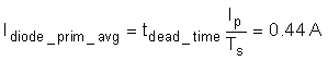
The RMS value of switch current is calculated from Figure 2-21 over a switching cycle. The diode conducts for only a small fraction of time during the switching period, as in, the dead time causing ZVS. The dead time chosen for this application is 200 ns.
From the data sheet of the SiC MOSFETs, the value of drain-source resistance corresponding to the applied gate voltage waveform is obtained. This value is approximately 20 mΩ. The forward voltage drop across the body diode is 4.2 V. The conduction losses across the four primary side FETs is calculated using Equation 22:

Similarly, the conduction losses are calculated across the secondary side FETs by scaling the primary side RMS currents with transformer turns ratio using Equation 23 and Equation 24. The on state resistance of the secondary side MOSFET is approximately 33 mΩ.


 Figure 2-21 Switch Current Waveforms for Calculating RMS Value of Current
To calculate switching losses, the switching loss curves from the manufacturer are used. Shown in Figure 2-22 and Figure 2-23 are the switching loss curves from manufacturer for the primary and secondary side FETs.
 Figure 2-22 C3M0030090K Loss Curves
 Figure 2-23 C3M0016120K Switching Curves
Because the FETs turn on at zero voltage, only the turn off loss coefficients are used for calculating the switching losses. Consider the secondary side MOSFETs for illustrating the calculation of switching losses. The curves are characterized during the double pulse test for a voltage of 600 V. From the graph, it can be inferred that at 50 A, the turn off energy is around 0.18 mJ. Using this information in Equation 25, the values of switching loss is obtained.
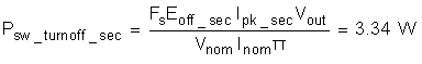
In Equation 25, Vout is the maximum secondary voltage at 500 V, Ipk_sec is the maximum current in the secondary at approximately 35 A, Fs is the switching frequency, Eoff_sec is the turn off loss coefficient, and Vnom and Inom are obtained from the data sheet. Similarly, the turn off loss across the primary is calculated in Equation 26.
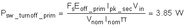
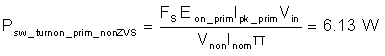
Total turn off switching losses in the primary and secondary side across all eight switches comes to 36 W. In addition to these losses, two switches of the primary turn on at non-zero voltage, leading to switching losses during turn. This is because the inductor stored energy (0.5 Li2) at this point is not fully sufficient to discharge the capacitive energy (0.5 CV2) at the output of the MOSFETs. These losses are calculated in the same way as calculated previously, but the turn on loss coefficients are taken. These losses come to approximately 24 W across both of the switches.