JAJU732C June 2019 – July 2022
- 概要
- Resources
- 特長
- アプリケーション
- 5
- 1System Description
- 2System Overview
- 3Circuit Description
- 4Hardware, Software, Testing Requirements, and Test Results
- 5Design Files
- 6Related Documentation
- 7Terminology
- 8About the Author
- 9Revision History
4.4.2 Lab 2
In the lab 2 build, the board is excited in open-loop fashion with a specified frequency (100 kHz) and phase shift. The phase shift can be changed through the watch window. The phase shift is controlled with the DAB_pwmPhaseShiftPrimSec_pu variable. This build verifies the sensing of feedback values from the power stage, operation of the PWM gate driver, HW protection, and ensures there are no hardware issues. Additionally, calibrate the input and output voltage sensing in this build.
- Test Setup for Lab 2
The hardware for this reference design is composed of the following boards:
- One TIDA-010054 power board
- Four TIDA-010054 gate driver cards
- Two TIDA-01606 ISOHV sense cards
- One TMDSCNCD280049C control card
- Mini USB cable
- Laptop
- The following test equipment is needed to
power and evaluate the DUT
- 10-kW DC source capable of delivering voltage between 700 V–800 V at required current
- 10-kW resistive load bank
- Power analyzer
- Dual channel +15-V, 4-V auxiliary bench power supply
- Oscilloscope
- Isolated voltage probes and current probe
Software Setup for Lab 2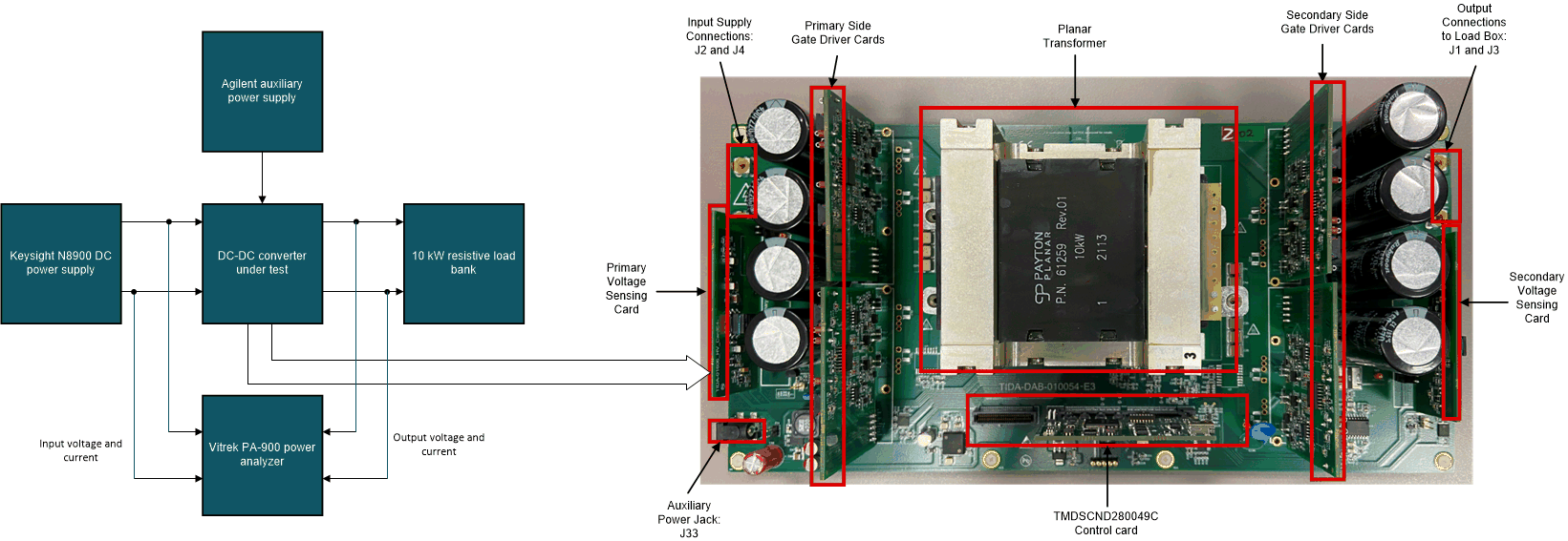 Figure 4-20 Lab 2 Test
Setup
Figure 4-20 Lab 2 Test
SetupThe following defines are set in the "settings.h" file for this build. The settings can be defined by selecting Lab 2: Open Loop PWM with Protection in the drop-down menu of Project Options from PowerSUITE GUI.
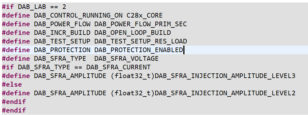 Figure 4-21 Lab 2 Software
Setup
Figure 4-21 Lab 2 Software
Setup- Run the project by clicking the green run button in CCS
- Populate the required
variables in the watch window by loading javascript '
setupdebugenv_lab2.js' in the scripting console
 Figure 4-22 Lab 2 Watch
View Configuration
 - Enable PWM by writing “1” to the DAB_clearTrip variable
- In the watch view, check
if the DAB_vPrimSensed_Volts, DAB_iPrimSensed_Amps,
DAB_vSecSensed_Volts, and DAB_iSecSensed_Amps variables are updating
periodicallyNote: Because no power is applied at this point, these are close to zero.
- Now, slowly increase the input VPRIM DC voltage from 0 V to 800 V. Make sure DAB_vPrimSensed_Volts displays the correct values.
- By default, the
DAB_pwmPhaseShiftPrimSec_pu variable is set to 0.032. Vary this phase
shift slowly in steps of 0.002 pu and observe the change in voltage at
the output of converter. Care must be taken to not increase the phase
shift very high as it can boost the output voltage greater than the
input voltage and can lead to breakdown of MOSFETs at maximum applied
voltage
.
- Measure SFRA Plant for Voltage Loop
- The SFRA is integrated in the C2000Ware-DigitalPower-SDK kit to measure the plant response which can then be used to design a compensator. Run the SFRA by clicking on the SFRA icon. The SFRA GUI opens.
- Select the options for the device on the SFRA GUI; for example, for F280049, select floating point. Click the Setup Connection button. In the pop-up window, uncheck the boot-on-connect option and select an appropriate COM port. Select the OK button. Return to the SFRA GUI and click the Connect button.
- The SFRA GUI connects to the device. A SFRA sweep can now be started by clicking the Start Sweep button. The complete SFRA sweep takes a few minutes to complete. Monitor the activity in the progress bar on the SFRA GUI or by checking the flashing blue LED on the back of the control card, which indicates UART activity.
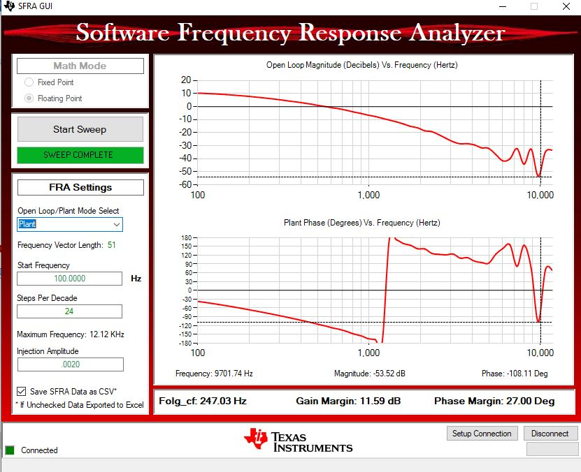 Test condition: VIN = 600 V, VOUT = 425 V, IIN = 4.72 A, Phase shift = 0.056, SFRA Amplitude = 0.002Figure 4-23 Lab 2 SFRA Plant Plot for the Open Voltage Loop Test
 - The Frequency Response Data ("SFRA.csv") is saved in the project folder, under an SFRA Data Folder, and is time-stamped with the time of the SFRA run. SFRA can be run at different frequency setpoints to cover the range of operation of the system. A compensator is designed using these measured plots through compensator designer.
Inside ISR1, the SFRA injects small signal perturbations in phase and observes the sensed output voltage variations. The following lines of code inside the dab.h file perform the SFRA signal injection and collection.
 Figure 4-24 Lab 2 Code for SFRA Signal Injection
- Measure SFRA Plant for Current Loop
- Follow the same steps as in voltage loop to get started with SFRA measurement for current loop.
- In the PowerSUITE GUI under SFRA tab, choose "current" prior to running the SFRA current loop.
 Figure 4-25 Lab 2 Code Defines SFRA Current Loop
 - Inside ISR1, the SFRA injects small signal perturbations in phase and observes the sensed output current variations. The following lines of code inside the dab.h file perform the SFRA signal injection and collection.
 Figure 4-26 Lab 2 Code for SFRA Signal Injection
 - Measure the plant response from SFRA GUI. The open loop and plant response are stored in the file named 'SFRA.csv'. Use this file to tune the compensator for the current loop.
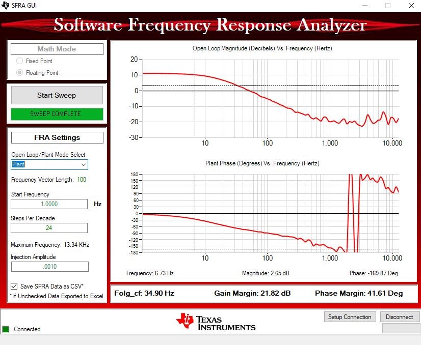 Figure 4-27 Lab 2 SFRA Plant Plot for the Open Current Loop TestNote: The current is sensed by AMC3301 at the battery (load) side
- Protection validation
The limits for overcurrent and overvoltage protection can be modified from PowerSUITE GUI.
#define DAB_ISEC_TRIP_LIMIT ((float32_t) 8.0)
#define DAB_IPRIM_TRIP_LIMIT ((float32_t) 1.5)
#define DAB_IPRIM_TANK_TRIP_LIMIT ((float32_t)35.0)
#define DAB_VSEC_TRIP_LIMIT ((float32_t)500)
Note: Secondary tank current and Primary overvoltage protection are not supported in the current HW.Set the limits to a lower value and adjust the source, the load, or both to exceed the thresholds to validate the trips.
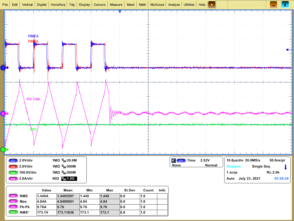 Primary - tank overcurrent protection, limit set = 4 AFigure 4-28 Lab 2 Primary - Tank Overcurrent Protection
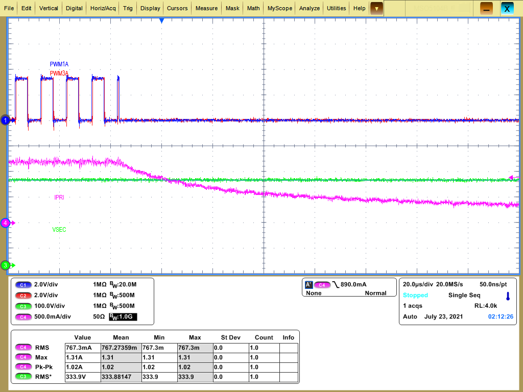 Primary (input) overcurrent protection, limit set = 1 AFigure 4-29 Lab 2 Primary (Input) Overcurrent Protection
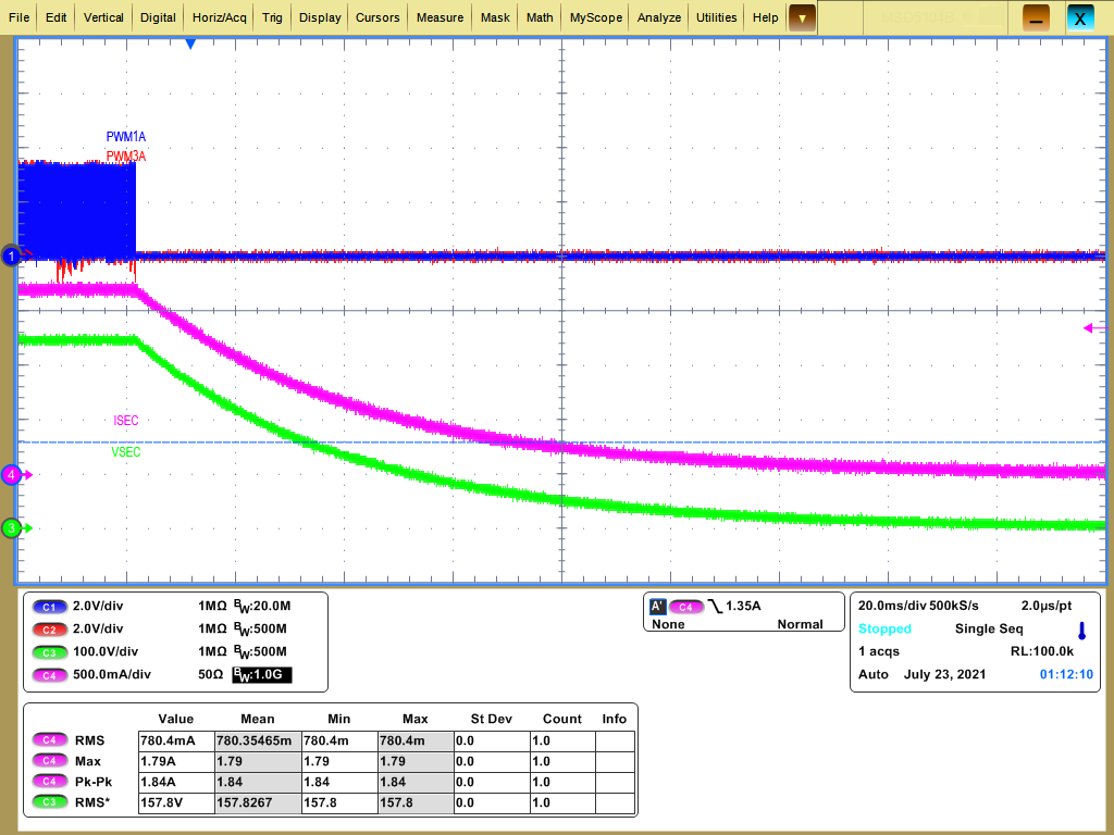 Secondary (resistive load) overcurrent protection, limit set = 1.5 AFigure 4-30 Lab 2 Secondary (Resistive Load) Overcurrent Protection
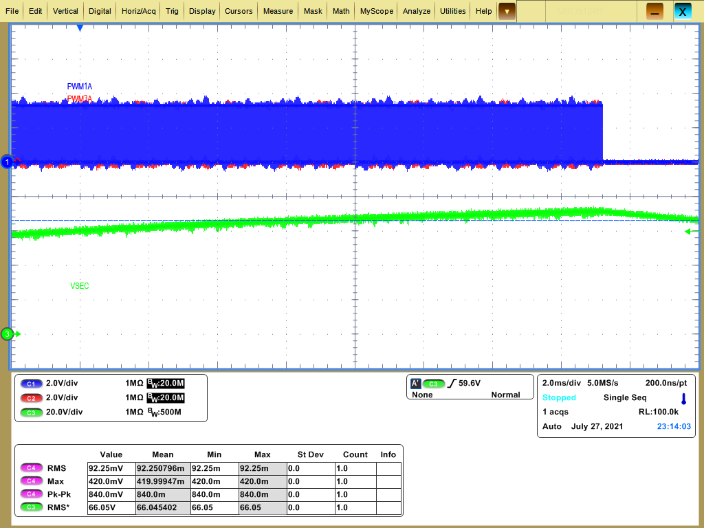 DAB_VSEC_TRIP_LIMIT = 75 VFigure 4-31 Lab 2 Secondary Overvoltage Protection
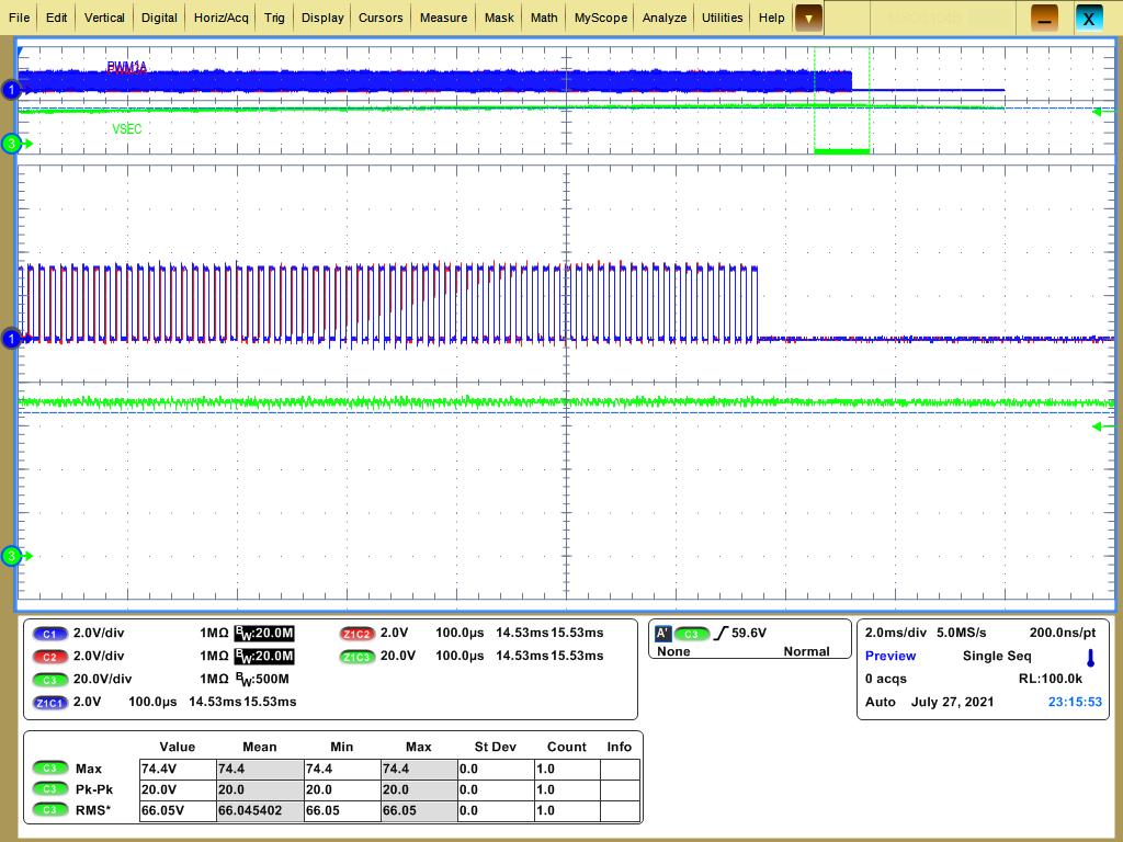 DAB_VSEC_TRIP_LIMIT = 75 V (Zoomed In)Figure 4-32 Lab 2 Secondary Overvoltage Protection(Zoomed In)
The previous waveforms show PWM is shut off by the comparator sub-system during fault events. The type of fault is displayed in the watch window (Figure 4-33) through variable "DAB_tripFlag". The trip can be reset by selecting "noTrip" under the drop-down menu and re-enabling the PWM by writing “1” to the DAB_clearTrip variable. Make sure the fault condition is removed before re-enabling the PWM.
 Figure 4-33 Lab 2-14