SNOA930C March   2015  – May 2021 LDC0851 , LDC1001 , LDC1001-Q1 , LDC1041 , LDC1051 , LDC1101 , LDC1312 , LDC1312-Q1 , LDC1314 , LDC1314-Q1 , LDC1612 , LDC1612-Q1 , LDC1614 , LDC1614-Q1 , LDC2112 , LDC2114 , LDC3114 , LDC3114-Q1


  1.   Trademarks
  2. 1The Sensor
    1. 1.1 Sensor Frequency
    2. 1.2 RS and RP
      1. 1.2.1 AC Resistance
      2. 1.2.2 Skin Effect
  3. 2Inductor Characteristics
    1. 2.1 Inductor Shape
      1. 2.1.1 Example Uses of Different Inductor Shapes
    2. 2.2 Number of Turns
    3. 2.3 Multiple Layers
      1. 2.3.1 Mutual Inductance of Coils in Series
      2. 2.3.2 Multi-Layer Parallel Inductor
      3. 2.3.3 Temperature Compensation
    4. 2.4 Inductor Size
    5. 2.5 Self-Resonance Frequency
      1. 2.5.1 Measurement of SRF
      2. 2.5.2 Techniques to Improve SRF for Wire-wound Inductors
  4. 3Capacitor Characteristics
    1. 3.1 Capacitor RS, Q, and SRF
    2. 3.2 Effect of Parasitic Capacitance
      1. 3.2.1 Recommended Capacitor Values
    3. 3.3 Capacitor Placement
  5. 4Physical Coil Design
    1. 4.1 Example Design Procedure Using WEBENCH
      1. 4.1.1 General Design Sequence
    2. 4.2 PCB Layout Recommendations
      1. 4.2.1 Minimize Conductors Near Sensor
      2. 4.2.2 Sensor Vias and Other Techniques for PCBs
  6. 5Summary
  7. 6References
  8. 7Revision History

Minimize Conductors Near Sensor

To keep the RP as high as possible, keep ground planes and any thick traces away from the sensor — minimize any conductors within at least 30% of the diameter of sensor. This includes ground planes and power planes. Do not place a ground pour around the sensor or use thieving on the board. In Figure 4-2, the ground pour on the inner tan layer has been recessed away from the coil to reduce coupling to the inner grounds.
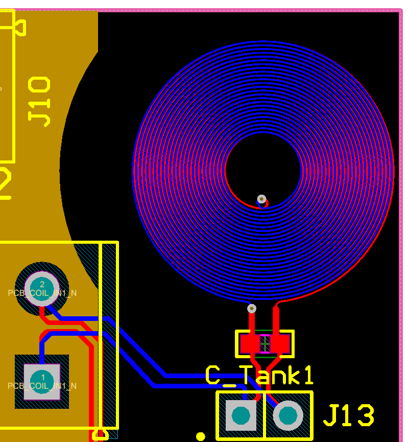
GUID-49B7CC9A-95DC-46E1-A046-F7698E0962AF-low.pngFigure 4-2 Minimize Copper Around the Sensor