SPRABJ8B September 2022 – November 2023 AM2631 , AM2631-Q1 , AM2632 , AM2632-Q1 , AM2634 , AM2634-Q1 , AM263P4
12.2.1 Key Layout Considerations
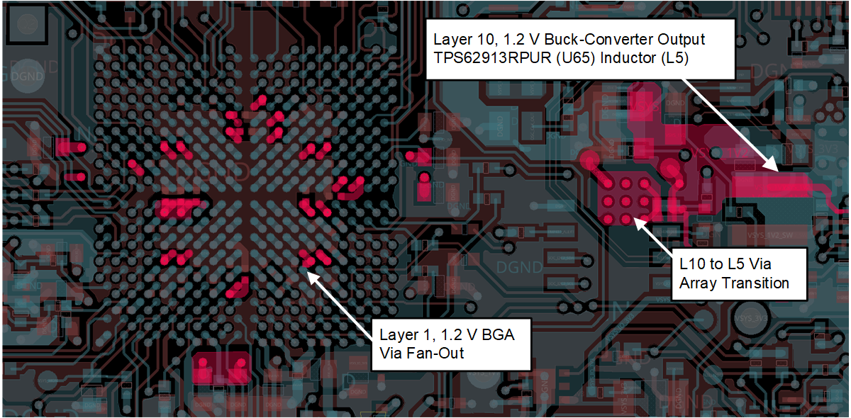
- AM263x or AM263Px should be co-located with the 1.2 V core digital regulator to allow for minimal IR drop from the regulator to the BGA power pins.
- Wide 15 mil traces should be used for all power and ground return via fan-out.
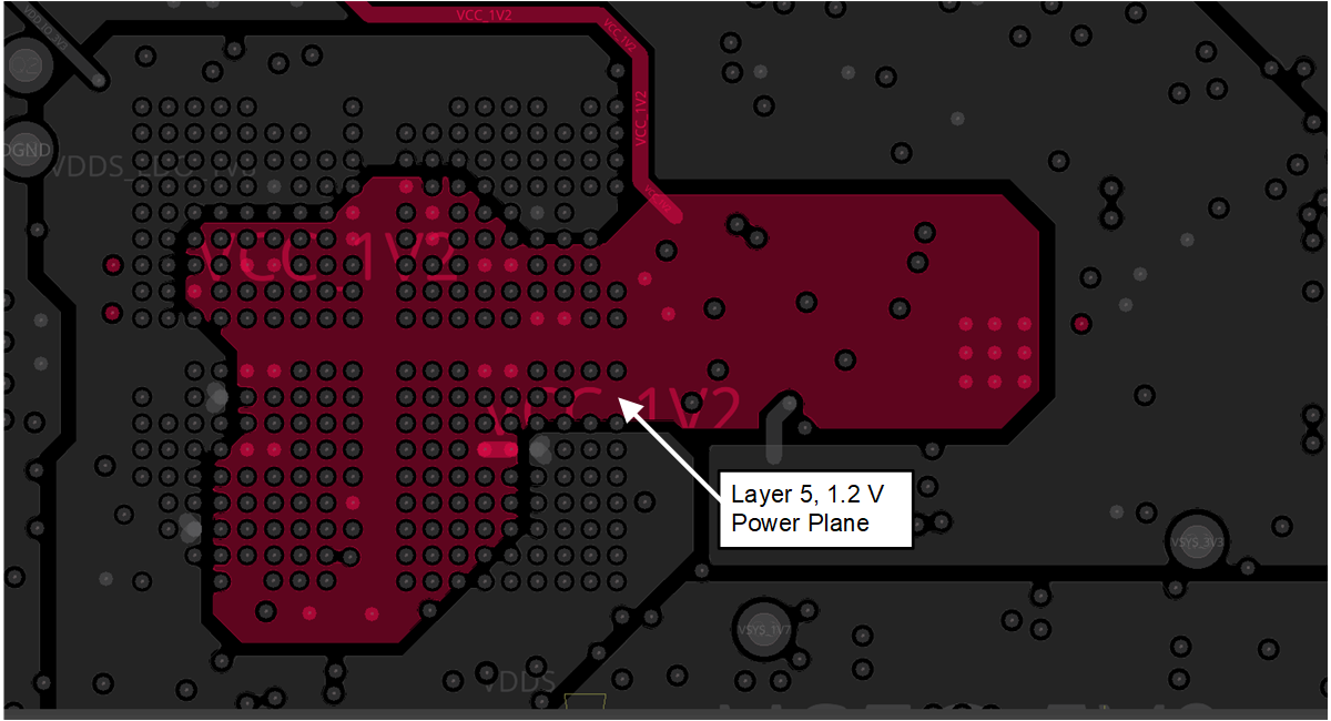
- A dedicated power layer, with tightly coupled ground return reference plane should be used for best transient performance and EMI coupling
- A wide power plane entry into the center of the BGA 1.2 V power pin areas should be used for minimal IR drop and best transient performance
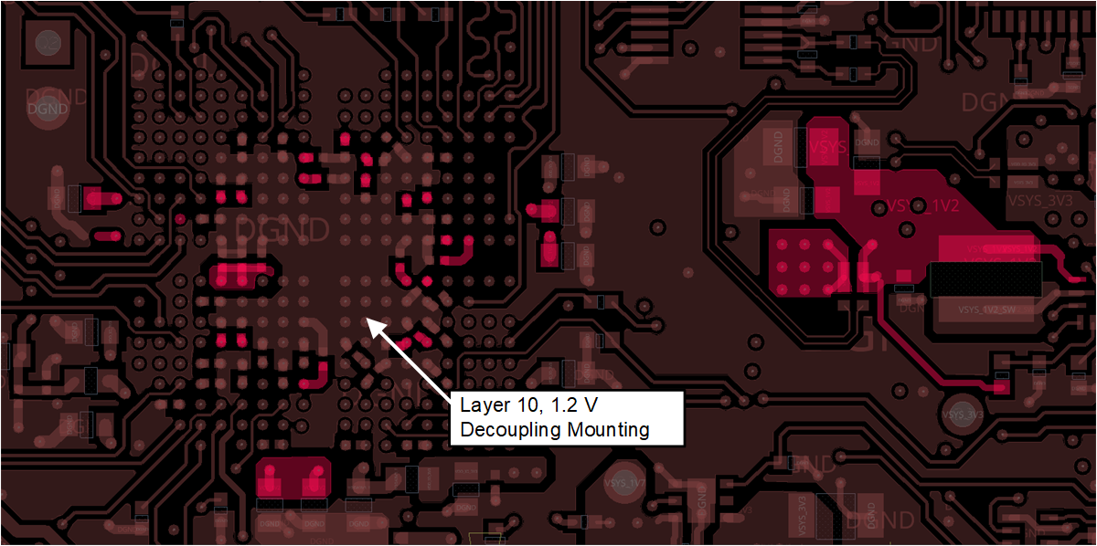
- Larger packaged, lower-frequency, bulk capacitance should be placed adjacent to the BGA with vias directly to power plane paths
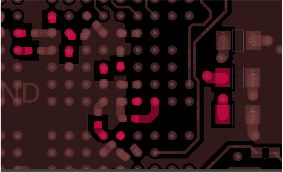
- Smaller packaged, higher-frequency decoupling capacitance should be placed directly on BGA fan-out vias with as small of a dog-bone to power and ground return vias as possible
 Figure 12-3 AM263x controlCARD Excerpt – 1.2 V Core Power Output, Power Plane Vias and BGA Vias
 Figure 12-4 AM263x controlCARD Excerpt – 1.2 V Core Power Plane, Layer 5
 Figure 12-5 AM263x controlCARD Excerpt – 1.2 V Core Power Decoupling Mounting, Layer 10
  Figure 12-6 AM263x controlCARD Excerpt – 1.2 V Core Power Decoupling Mounting, Layer 10