SPRABJ8B September 2022 – November 2023 AM2631 , AM2631-Q1 , AM2632 , AM2632-Q1 , AM2634 , AM2634-Q1 , AM263P4
2.5.1.1 Core Digital Power 1.2 V
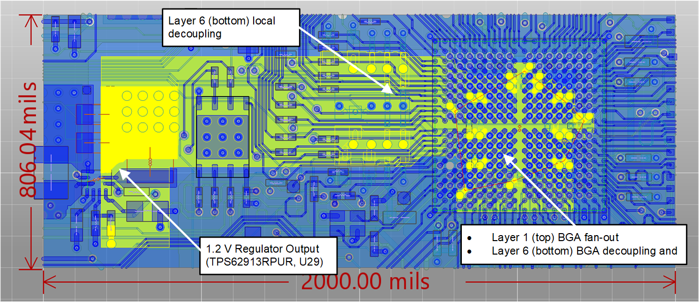
Z11 simulations were performed on the 1.2 V core digital power net of the LP-AM263 LaunchPad EVM to verify transient power margin. The simulation domain included the:
- AM263x BGA (UI) 1.2 V digital and GND return fan-out
- Internal PCB 1.2 V and GND return planes
- Decoupling placed on the 1.2 V power net,
- U29 buck regulator output LC filter up to switch node
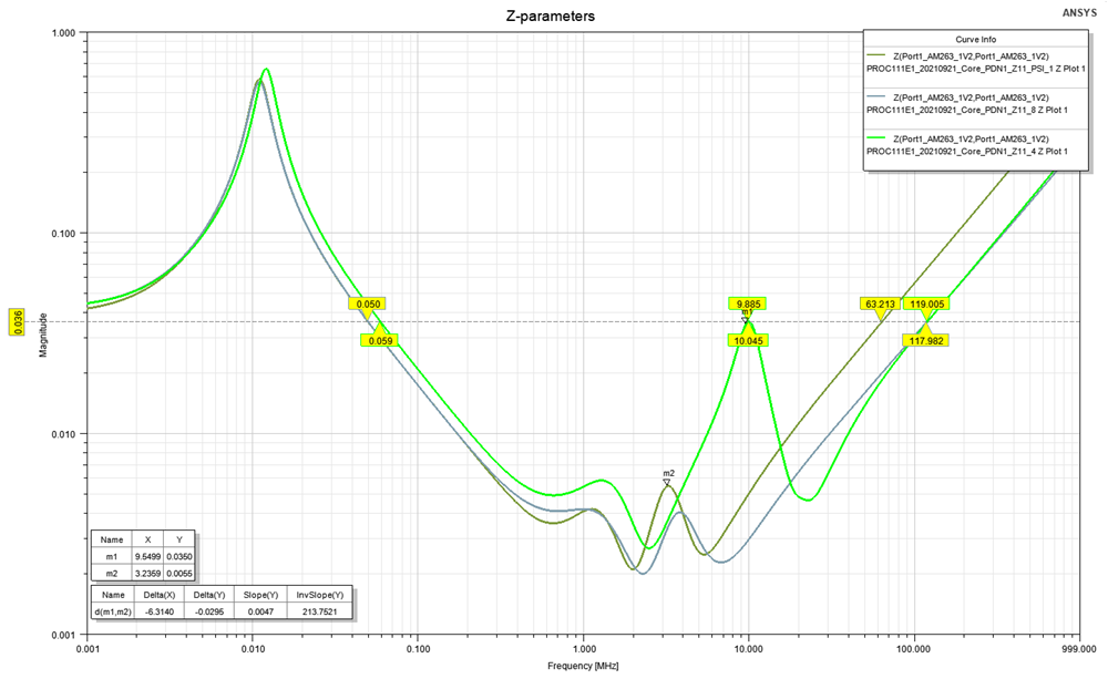
These simulations were done iteratively with multiple capacitor BOM changes made between each iteration. Each iteration was characterized primarily by the maximum and minimum frequency bandwidth below Ztarget (see above sections) and the BOM selection changed to maximize bandwidth and maximum Ztarget margin. Only the initial and final chosen BOM iterations are shown in Figure 2-12 and Figure 2-13.
 Figure 2-12 AM263x LaunchPad PDN Simulations – 1.2 V Core Power Simulation Domain
  Figure 2-13 AM263x LaunchPad PDN Simulations – 1.2 V Core Power Simulated Z11
- AM263x LaunchPad PDN Simulations – 1.2 V Core Power Simulated Z11
- This resulted in the marker (m2) point of 5.5 mΩ
- Ztarget requirement of 36mOhm maintained from 50 KHz to 63 MHz
- Major difference in BOM was replacing all 0.1 µF BGA and local decoupling capacitors with 1.0 µF capacitors this entirely removed the 10 MHz resonant point in the PDN impedance spectrum
- PROC111E1_20210921 Initial simulations
- Major resonance at 10 MHz eliminated almost all margin against 36 mΩ Ztarget requirement