SPRABJ8B September 2022 – November 2023 AM2631 , AM2631-Q1 , AM2632 , AM2632-Q1 , AM2634 , AM2634-Q1 , AM263P4
2.3 Power Decoupling and Filtering
Table 2-1 describes the initial BGA decoupling and power filtering required for the AM263x and AM263Px. These were based on the initial simulation feedback of the Control Card EVM PCB and AM263x package with the transient use-cases shown in Table 2-3.
The decoupling network presented in the below sections and in the AM263x EVM schematics and layouts are reasonable starting points for any AM263x or AM263Px PCB design. However, due to specific PCB routing differences and the resulting plane capacitance and decoupling mounting inductances and other parasitics, it is highly recommended that designers simulate and measure their specific power distribution network performance. Simulations and measurements should ideally be done with target application software active, and intended operating environment conditions applied to the system.
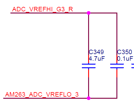
The AM263Px Sensor Package has additional set of ADC reference voltages, ADC_VREFHI_G3 and ADC_VREFLO_G3, which are shown in Figure 2-10
| Device Supply | Quantity | Comment | Part Number | Manufacturer |
|---|---|---|---|---|
| VDD_CORE | 2 | 2.2 µF, 6.3 V, ± 10%, X7R, AEC-Q200 Grade 1, 0603 | GCM188R70J225KE22D | Murata |
| 3 | 0.22 µF, 16 V,± 10%, X7R, AEC-Q200 Grade 1, 0402 | GCM155R71C224KE02D | Murata | |
| 16 | 0.01 µF, 50 V, ± 10%, X7R, AEC-Q200 Grade 1, 0402 | CGA2B3X7R1H103K050BB | TDK | |
| VNWA | 1 | 0.22 µF, 16 V, ± 10%, X7R, AEC-Q200 Grade 1, 0402 | GCM155R71C224KE02D | Murata |
| 1 | 0.01 µF, 50 V, ± 10%, X7R, AEC-Q200 Grade 1, 0402 | CGA2B3X7R1H103K050BB | Murata | |
| VDD_F | 1 | 0.22 µF, 16 V, ± 10%, X7R, AEC-Q200 Grade 1, 0402 | GCM155R71C224KE02D | TDK |
| 1 | 0.01 µF, 50 V, ± 10%, X7R, AEC-Q200 Grade 1, 0402 | CGA2B3X7R1H103K050BB | TDK | |
| VDDAR_CORE | 1 | 2.2 uF, 6.3 V, ± 10%, X7R, AEC-Q200 Grade 1, 0603 | GCM188R70J225KE22D | Murata |
| 2 | 0.22 µF, 16 V,± 10%, X7R, AEC-Q200 Grade 1, 0402 | GCM155R71C224KE02D | Murata | |
| 1 | Ferrite Bead, 120 Ω @ 100 MHz, 2 A, 0603 | 742792625 | Wurth | |
| 3 | 0.01 µF, 50 V, ± 10%, X7R, AEC-Q200 Grade 1, 0402 | CGA2B3X7R1H103K050BB | TDK | |
| VDDA18_LDO VDDA18 VDDA18_OSC_PLL VDDA18_TEMP |
1 | 3.3 µF, 10 V, ± 10%, X5R, 0603 | GRM188R61A335KE15D | Murata |
| 4 | 0.1 µF, 6.3 V, ± 10%, X7R, 0402 | GRM155R70J104KA01D | Murata | |
| VDDS18_LDO VDDS18 |
1 | 3.3 µF, 10 V, ± 10%, X5R, 0603 | GRM188R61A335KE15D | Murata |
| 4 | 0.1 µF, 6.3 V, ± 10%, X7R, 0402 | GRM155R70J104KA01D | Murata | |
| VDDS33 | 3 | 2.2 µF, 6.3 V, ± 10%, X7R, AEC-Q200 Grade 1, 0603 | GCM188R70J225KE22D | Murata |
| 4 | 0.22 µF, 16 V, ± 10%, X7R, AEC-Q200 Grade 1, 0402 | GCM155R71C224KE02D | Murata | |
| 1 | Ferrite Bead, 120 Ω @ 100 MHz, 2 A, 0603 | 742792625 | Wurth | |
| 7 | 0.01 µF, 50 V, ± 10%, X7R, AEC-Q200 Grade 1, 0402 | CGA2B3X7R1H103K050BB | TDK | |
| VDDA33 | 1 | 2.2 µF, 6.3 V, ± 10%, X7R, AEC-Q200 Grade 1, 0603 | GCM188R70J225KE22D | Murata |
| 2 | 0.22 µF, 16 V, ± 10%, X7R, AEC-Q200 Grade 1, 0402 | GCM155R71C224KE02D | Murata | |
| 1 | Ferrite Bead, 120 Ω @ 100 MHz, 2 A, 0603 | 742792625 | Wurth | |
| 3 | 0.01 µF, 50 V, ± 10%, X7R, AEC-Q200 Grade 1, 0402 | CGA2B3X7R1H103K050BB | TDK |
 Figure 2-6 AM263x LaunchPad Excerpt – 1.2
V Power Decoupling Schematic
  Figure 2-7 AM263x LaunchPad Excerpt – 3.3
V Digital I/O and Analog I/O Decoupling and Filtering Schematic
  Figure 2-8 AM263x LaunchPad Excerpt – 1.8
V Digital I/O and Analog I/O Decoupling and Filtering Schematic
 Figure 2-9 AM263x LaunchPad Excerpt – ADC
and DAC VREF Decoupling Schematic
 Figure 2-10 AM263Px controlCard Excerpt –
additional VREFHI_G3 and VREFLO_G3 connections