SPRABJ8B September 2022 – November 2023 AM2631 , AM2631-Q1 , AM2632 , AM2632-Q1 , AM2634 , AM2634-Q1 , AM263P4
12.4.1 Key Layout Considerations
- Wide, minimum 15 mil traces, should be used for all power and ground return via fan-out.
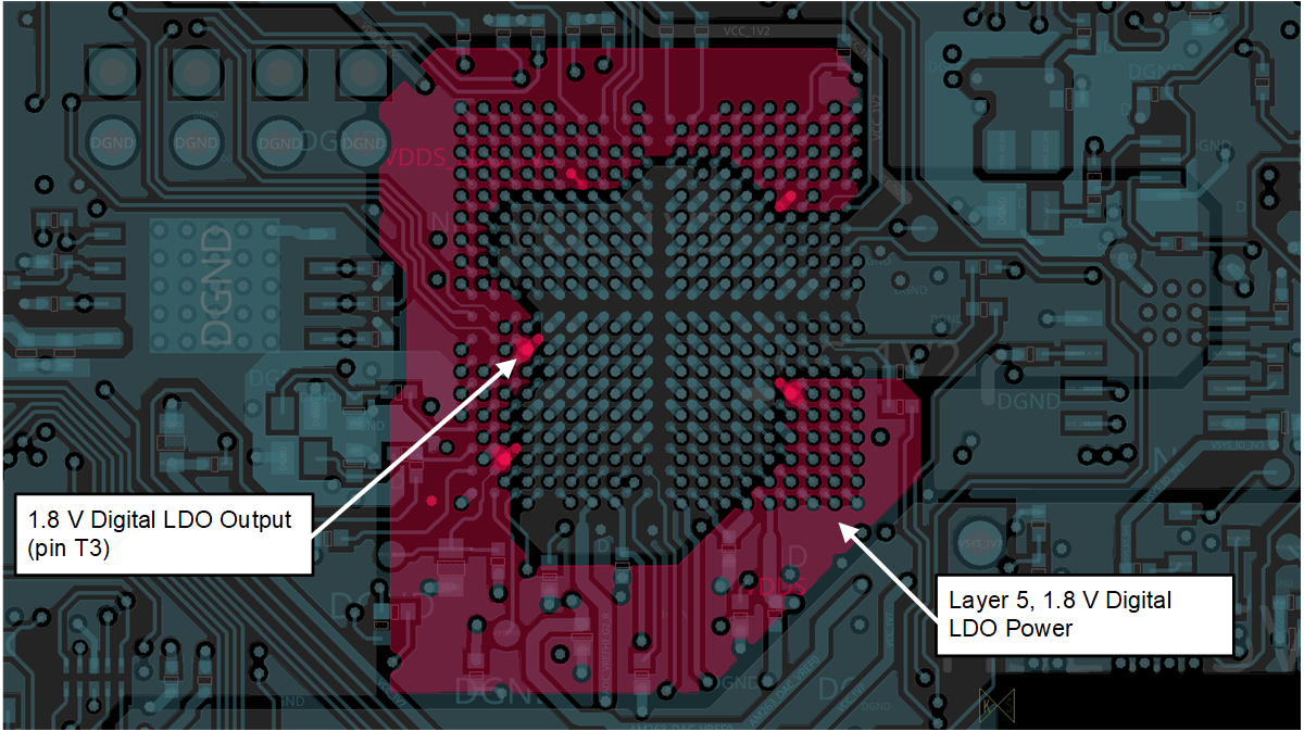
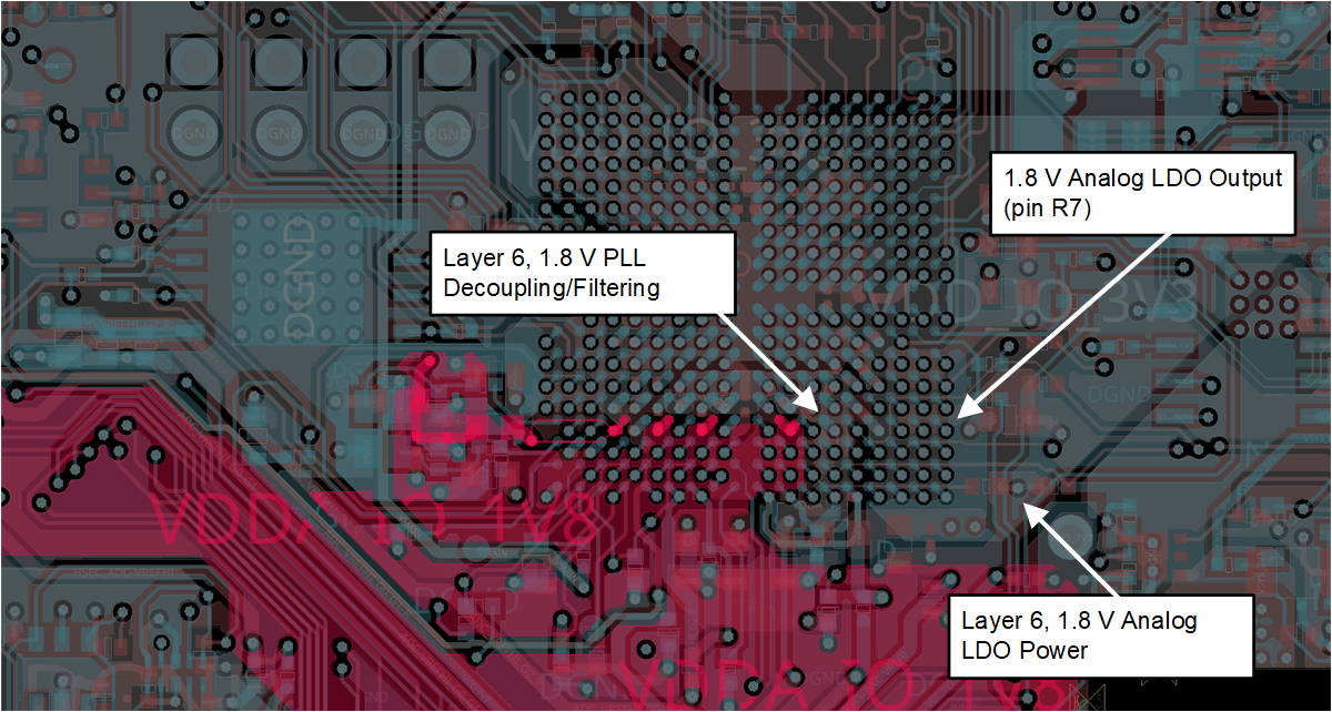
- 1.8 V digital and analog is generated from on-chip LDO and so is highly localized to the BGA pinout
- A tightly coupled, adjacent ground return reference plane should be used for best transient performance and EMI coupling
- Smaller power planes or wider traces should be used for minimal IR drop and best transient routing across the associated BGA pins
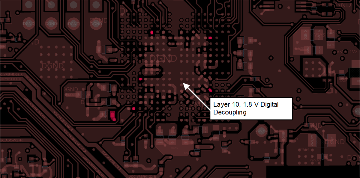
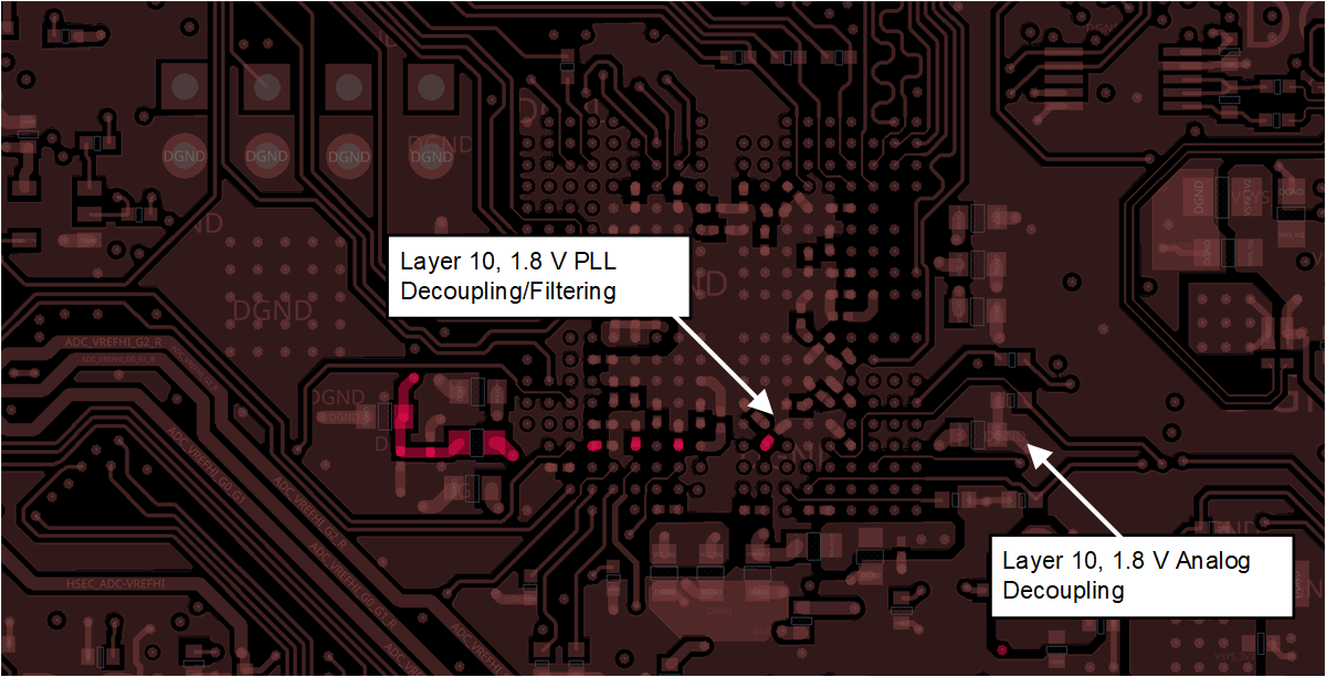
- Smaller packaged, higher-frequency decoupling capacitance should be placed directly on BGA fan-out vias with as small of a dog-bone to power and ground return vias as possible
 Figure 12-12 AM263x controlCARD Excerpt – 1.8 V Digital Power Via Fan-Out and Plane Routing Layer 6
 Figure 12-13 AM263x controlCARD Excerpt – 1.8 V Digital Power Decoupling on Layer 10
 Figure 12-14 AM263x controlCARD Excerpt – 1.8 V Analog Power Via Fan-Out and Plane Routing Layer 6
Note: Figure 2-13 shows an example of a suboptimal routing between the FL12 filter output and the BGA pads. Ideally the output of the FL12 filter should be routed as a wide trace or small plane, and not smaller traces as was done on this initial revision of the controlCard EVM.
 Figure 12-15 AM263x controlCARD Excerpt – 1.8 V Analog Power Decoupling on Layer 10