SWRA726 March 2022 CC1120 , CC1121 , CC1201 , CC1310 , CC1311P3 , CC1311R3 , CC1312PSIP , CC1312R , CC1312R7 , CC1314R10 , CC1350 , CC1352P , CC1352R , CC1354P10 , CC1354R10 , CC2340R5-Q1 , CC2640R2L , CC2651R3 , CC2652P , CC2652P7 , CC2652R , CC2652R7 , CC2652RB , CC2652RSIP , CC3130 , CC3135MOD , CC3230S , CC3235MODAS , CC3235MODASF , CC3235MODSF , CC3235S , WL1801MOD , WL1805MOD , WL1807MOD , WL1831 , WL1831MOD , WL1835MOD , WL1837MOD
- Trademarks
- 1Introduction
- 2Antenna Standing Wave Ratio (SWR) Measurement
- 3Evaluation Board Matching Components Location
- 4Volpert-Smith Chart
- 5868-MHz PCB Helix Antenna Measurement and Matching
- 62.4-GHz PCB Compact Antenna Measurement and Matching
- 7 2.4-GHz PCB Inverted-F Antenna Measurement and Matching
- 8Fast in-circuit or in-device Antenna Verification
- 9Conclusion
4.2 Custom Calibration for 50-Ohm Load
Making a good quality calibration standard (open, short and matched loads) is not a trivial task, especially on PCB. Manufacturing of fixed broadband 50 Ohm load is very difficult (even a coaxial load).
For VNA calibration on PCB the standard SMD resistor and jumper is commonly used. Better to use thin film resistors. They are usually made on ceramic (or Al2O3) substrate with relatively stable dielectric constant over the wide frequency range. There are special UHF resistors with operation frequencies up to 50 GHz having very low reactance if connected properly.
Modern SMD thin film resistors and jumpers can be used in high frequency circuits, but they have some specific nuances over the wide operation frequency range. In addition, traces and vias on PCB add parasitic elements, for example, short via from bottom to top side can be considered as a small value inductor. For low frequencies this inductance is invisible, but with higher frequencies it starts to play a big role and can change circuit’s behavior. Configurations of traces with ratio to wavelength can have inductive or capacitive modes or can transform the impedances.
The SMD resistor at high frequency has an equivalent circuit as an active resistance in series with a small inductance and a shunt capacitor to both resistor’s pads. A parasitic inductance of the resistor is about 0.7…1.0 nH, the parasitic capacitance is about 0.1 pF. These are average values and depend on many factors. For low value resistors the parasitic inductance dominates and increases with frequency. For high value resistors, the parasitic capacitance dominates and is much higher than the parasitic inductance. For values from 50 to 100 Ohm of the standard SMD thin film resistors the operation frequency can be up to several GHz without a significant impedance changing.
A main question of calibration quality on PCB for antenna measurement and matching is: what's the real impedance and S11 parameter of the matched load (50 Ohm resistor)? Other words, what is the best and most accurate S11 (SWR) level can be measured. As an example, a Figure 4-5 shows S11 return loss values of the standard calibration kit at 868 MHz and 2440 MHz frequencies (precision 50 Ohm load).
A standard calibration kit has very high precise connectors with very predictable mechanical and electrical parameters (this is a reason why they are so expensive). It is possible to make a custom calibration kit, but many nuances have to be considered, so even quality of soldering and connectors repeatability can affect S11 value.
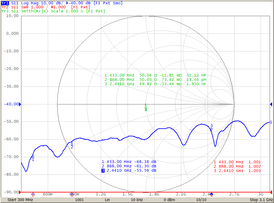 Figure 4-5 S11 Values of the Precision
Standard Calibration Kit at 868 MHz And 2440 MHz
Figure 4-5 S11 Values of the Precision
Standard Calibration Kit at 868 MHz And 2440 MHzS11 value at 868 MHz is -61.30 dB and corresponding SWR value is 1:1.002. At 2.441 GHz SWR value is 1:1.003. Meaning, after the calibration users can measure antenna SWR levels starting from 1:1.002 or 1:1.003, but not below these two levels at corresponding frequencies.
There are two methods of VNA calibration for taking the antenna measurements:
- Using the standard calibration kit, short pigtail (or cable) and port extension option.
- Using on-board calibration with open, short and matched 50 Ohm loads (SOL calibration).
The standard calibration kits are expensive, so the method of on-board calibration is more popular, but less precise.
Performing on-board calibration for in-device antenna matching brings users compromises as it’s impossible to make a precision open, short and matched loads due to parasitic elements. Users decide what is the compromise between a time being spent on board and equipment preparation for the calibration and final measured and matched results.
Below are three examples of measured 50 Ohm loads:
- Single 0402 size resistor 49.9 Ohm 0.1% (A)
- Two 0402 size resistors 100 Ohm 1% in shunt placed on top of each other (B)
- Two 0402 size resistors 100 Ohm 1% in shunt T-placement configuration (C)
The first example is shown for a single 49.9 Ohm 0.1% resistor (Figure 4-6). Measured S11, SWR and impedance are shown on Figure 4-7.
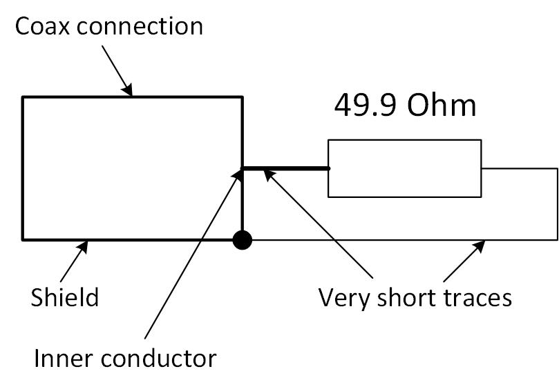 Figure 4-6 Single 49.9 Ohm Resistor
Connection
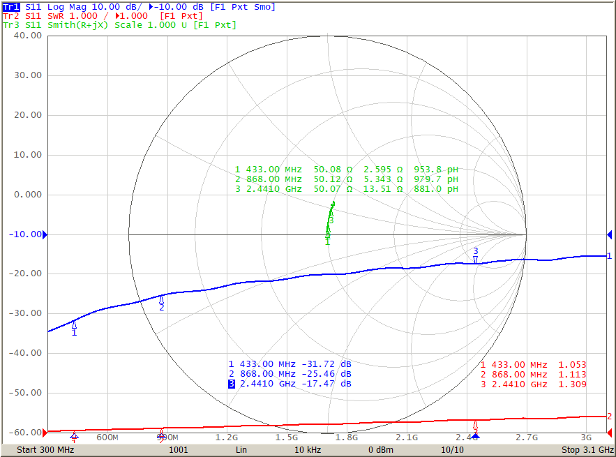 Figure 4-7 Measured Single 49.9 Ohm SMD
Resistor
Figure 4-7 Measured Single 49.9 Ohm SMD
ResistorAt 2.441 GHz the level of S11 is -17.36 dB. This means, the corresponding SWR value is 1:1.314.If VNA was calibrated with this matched load, users were unable to measure SWR below 1.314 level.
It happens due to a fact, the parasitic inductance in series with the active resistance increases with the frequency and adds about 13.51 Ohm at 2.441 GHz (Marker 3, Figure 4-7) making the total load’s (resistor’s) impedance (Z) = 51.86 Ohm. That is why users see SWR of 1:1.314.
Connecting two 100 Ohm 1% resistors in shunt and placing them on top of each other (Figure 4-8) decreases parasitic series inductance almost in double (Figure 4-9) down to 7.51 Ohm and 489 pH.
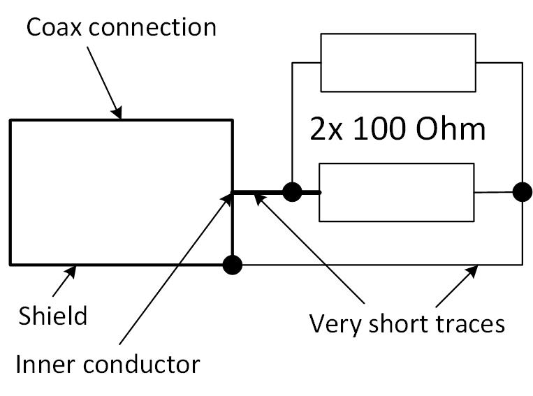 Figure 4-8 Two 100 Ohm Resistors in Shunt
Placed on Top of Each Other
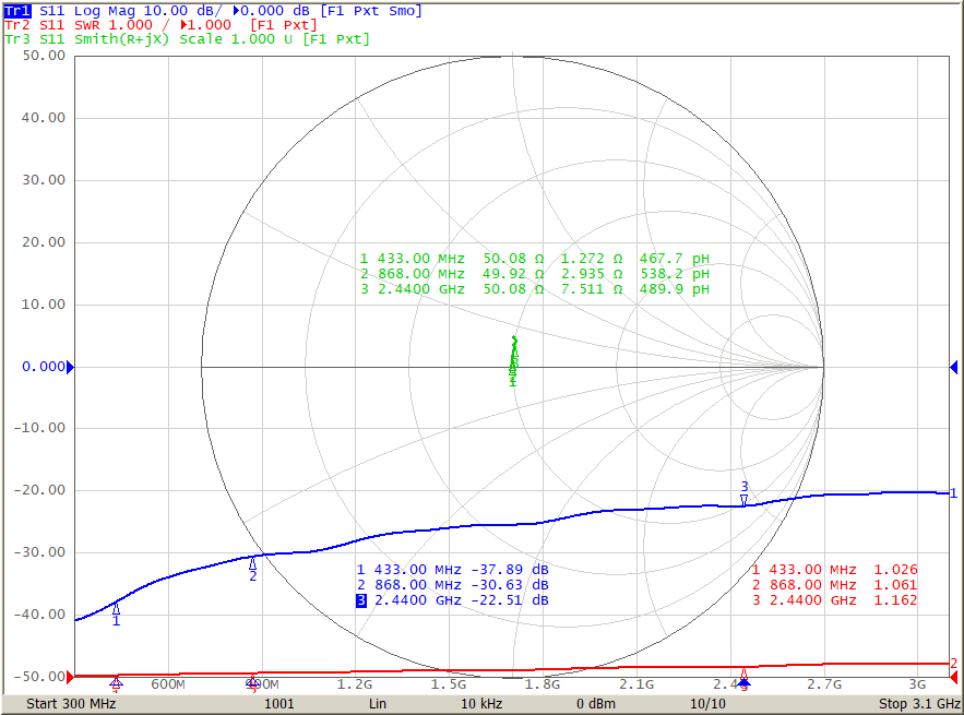 Figure 4-9 Measured Two 100 Ohm Resistors
in Shunt Placed on Top of Each Other
Figure 4-9 Measured Two 100 Ohm Resistors
in Shunt Placed on Top of Each OtherMeasured S11 values are shown on Figure 4-9. S11 improved down to - 22.51 dB with the corresponding SWR value of 1:1.162 at 2.441 GHz frequency.
Resistors T-placement configuration (Figure 4-10) gives highest accuracy, but requires a very short and solid ground plane with proper termination. Measured impedances and S11 levels are shown on Figure 4-11.
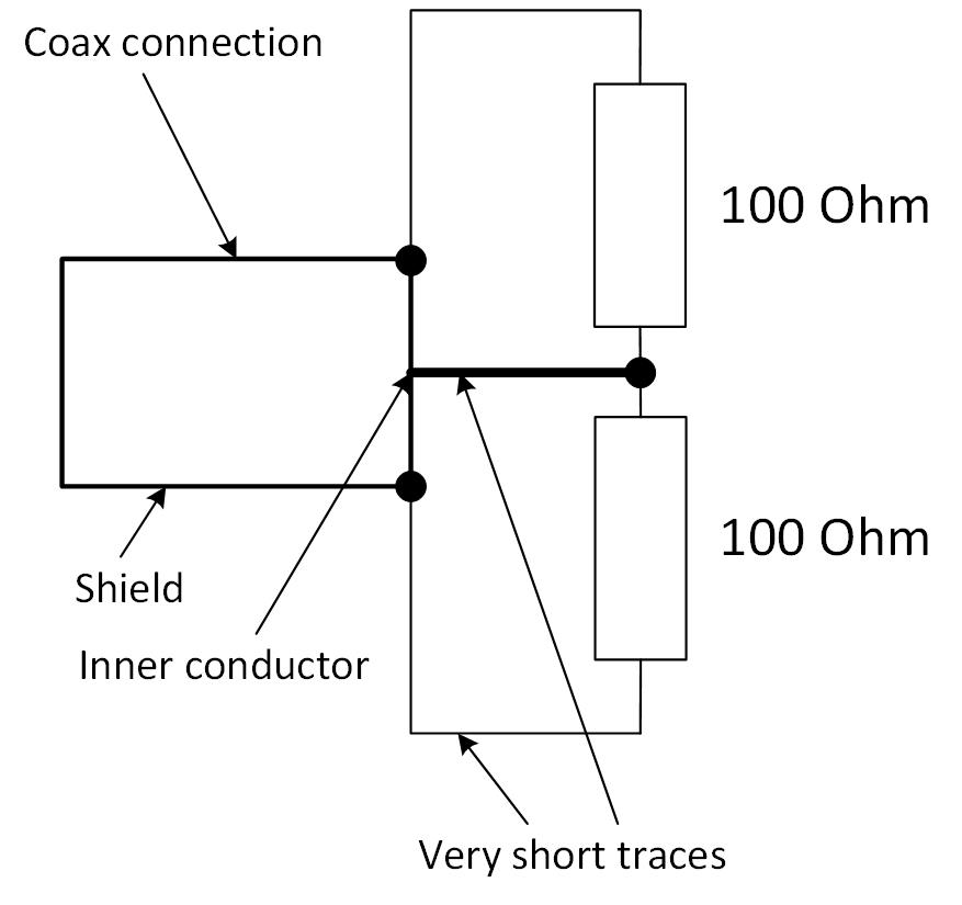 Figure 4-10 Resistors T-Placement
In reality such configuration is possible on PCB, but requires high quality cable connection to the board and short lines (matched traces) with a good, short and solid ground plane as a current return path. This means, for low power transceivers and real traces with their configuration on PCB it’s almost impossible to implement.
Users can place the resistors on PCB in such configuration, but it will not bring any valuable improvements in comparison to two 100 Ohm resistors in a shunt scheme placed on top of each other.
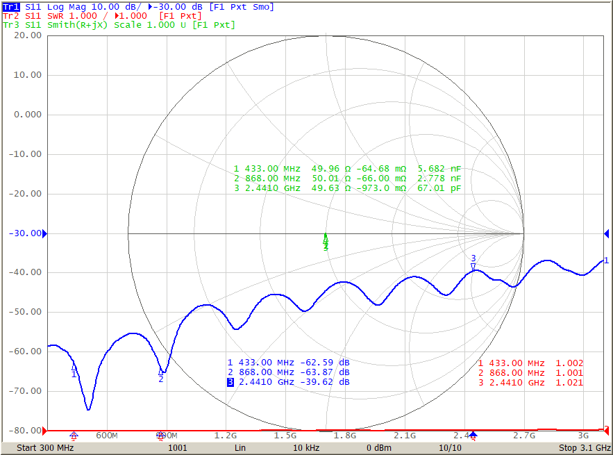 Figure 4-11 Measured Two 100 Ohm Resistors
in Shunt in T-Placement
Figure 4-11 Measured Two 100 Ohm Resistors
in Shunt in T-PlacementCorresponding SWR level to S11 value of - 39.62 dB is 1:1.021 at 2440 MHz (marker 3). It’s a decently good level for the custom 50 Ohm load.
Precise and matched to 50 Ohm load allows users to measure the lowest SWR value. Less precise load can offset SWR level and make possible VNA to measure SWR value higher than it is.
Figure 4-12 and Figure 4-13 show SWR and S11 parameters for the 868 MHz antenna measured at the same operation environment conditions, but VNA calibrations were made using loads (A) and (C) from the examples above.
Users can see, less precise load gives the highest measured SWR value of the antenna (1:1.636 versus 1:1.457).
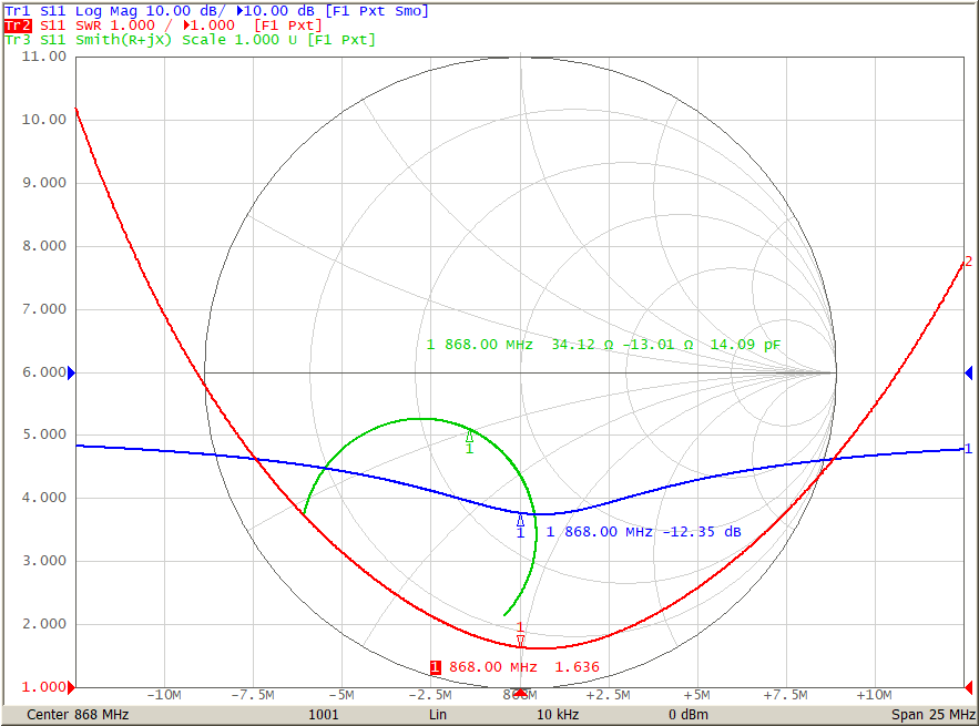 Figure 4-12 Measured Results After VNA
Calibration Using Load (A)
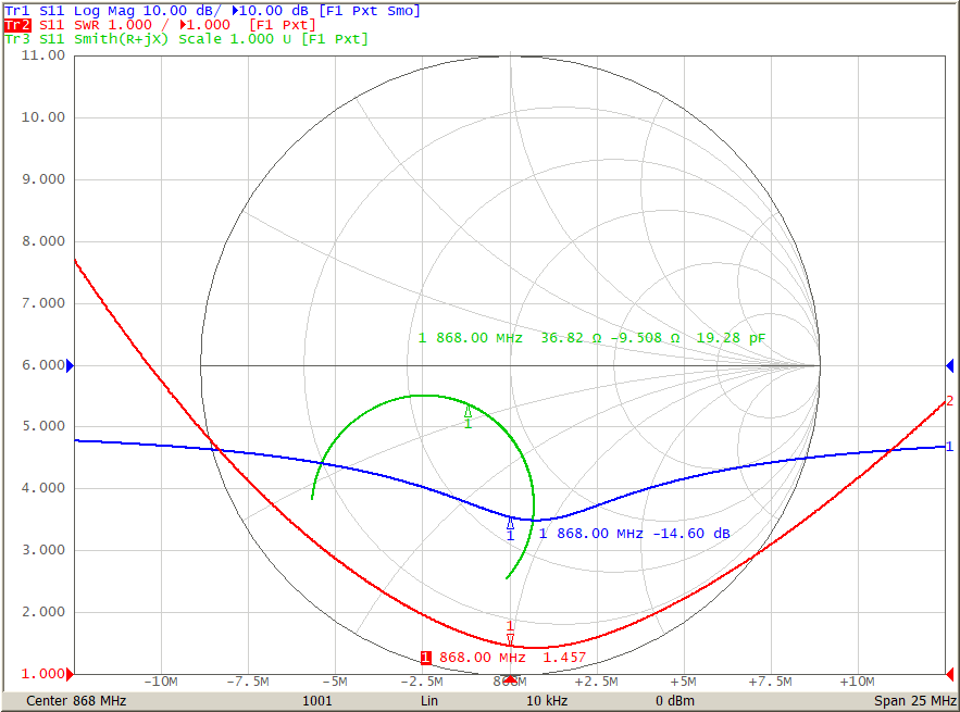 Figure 4-13 Measured Results After VNA
Calibration Using Load (C)
Figure 4-13 Measured Results After VNA
Calibration Using Load (C)Interesting to understand, that calibration load’s quality can affect a precise load measurement. Because VNA is thinking, that he was calibrated with a reference load and compares this reference to other loads. This means, the most precision load can be measured as having worst parameters. And this how the VNA operates. If users want to get most accurate measurements, VNA should be calibrated with the most precision load.
An example of such VNA operation is shown on Figure 4-14. VNA was calibrated by the load from the above example (A). The loads (B) and (C) were measured for S11. Users can see, the most accurate load (C) measured as having worst S11 parameter.
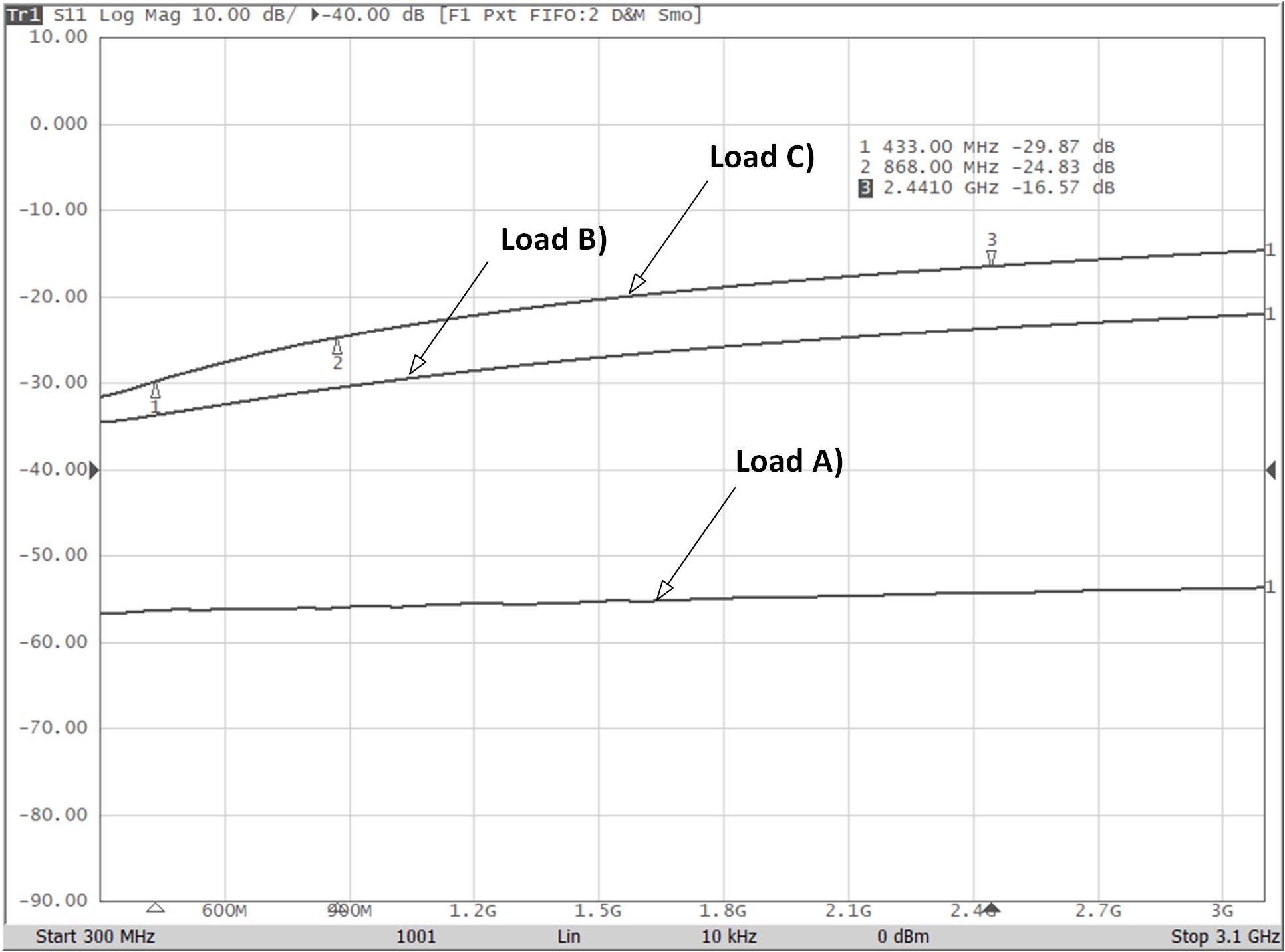 Figure 4-14 Loads S11 Parameter
Measurements
Figure 4-14 Loads S11 Parameter
MeasurementsMaking the custom calibration loads can be sufficient for frequencies up to 6 GHz. But many nuances have to be considered. Main question is how and to what the custom calibration loads can be compared. Precision calibration kit can help to answer this question.
If users don’t have an access to the precision calibration kit, the on-board calibration can be sufficient in many cases for proper antenna matching, but users need to pay attention to cable and soldering quality. In addition, proper layout techniques can help to decrease the parasitics.