SLVS348N July   2001  – January 2025 TPS793

PRODUCTION DATA  

  1.   1
  2. Features
  3. Applications
  4. Description
  5. Pin Configuration and Functions
  6. Specifications
    1. 5.1 Absolute Maximum Ratings
    2. 5.2 ESD Ratings
    3. 5.3 Recommended Operating Conditions
    4. 5.4 Thermal Information
    5. 5.5 Electrical Characteristics
    6. 5.6 Typical Characteristics
  7. Detailed Description
    1. 6.1 Overview
    2. 6.2 Functional Block Diagrams
    3. 6.3 Feature Description
      1. 6.3.1 Undervoltage Lockout (UVLO)
      2. 6.3.2 Shutdown
      3. 6.3.3 Active Discharge (new chip)
      4. 6.3.4 Foldback Current Limit
      5. 6.3.5 Thermal Protection
      6. 6.3.6 Reverse Current
    4. 6.4 Device Functional Modes
      1. 6.4.1 Normal Operation
      2. 6.4.2 Dropout Operation
      3. 6.4.3 Disabled
  8. Application and Implementation
    1. 7.1 Application Information
      1. 7.1.1 Adjustable Operation
      2. 7.1.2 Exiting Dropout
    2. 7.2 Typical Application
      1. 7.2.1 Design Requirements
      2. 7.2.2 Detailed Design Procedure
        1. 7.2.2.1 Capacitor Recommendations
        2. 7.2.2.2 Input and Output Capacitor Requirements
        3. 7.2.2.3 Noise Reduction and Feed-Forward Capacitor Requirements
      3. 7.2.3 Application Curves
    3. 7.3 Best Design Practices
    4. 7.4 Power Supply Recommendations
    5. 7.5 Layout
      1. 7.5.1 Layout Guidelines
        1. 7.5.1.1 Board Layout Recommendations to Improve PSRR and Noise Performance
        2. 7.5.1.2 Power Dissipation
      2. 7.5.2 Layout Example
  9. Device and Documentation Support
    1. 8.1 Device Support
      1. 8.1.1 Development Support
        1. 8.1.1.1 Evaluation Modules
        2. 8.1.1.2 Spice Models
      2. 8.1.2 Device Nomenclature
    2. 8.2 Documentation Support
      1. 8.2.1 Related Documentation
    3. 8.3 Receiving Notification of Documentation Updates
    4. 8.4 Support Resources
    5. 8.5 Trademarks
    6. 8.6 Electrostatic Discharge Caution
    7. 8.7 Glossary
  10. Revision History
  11. 10Mechanical, Packaging, and Orderable Information

Typical Characteristics

over recommended operating temperature range, TJ = –40°C to +125°C VEN = VIN, VIN = VO(typ) + 1V IOUT = 1mA, COUT = 10µF, CNR = 0.01µF (legacy chip) (unless otherwise noted); all typical values at TJ= 25°C
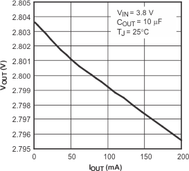
TPS793 TPS793 Output Voltage vs Output Current
Legacy chip
Figure 5-1 TPS793 Output Voltage vs Output Current
TPS793 TPS793 Output Voltage vs Junction Temperature
Legacy chip
Figure 5-3 TPS793 Output Voltage vs Junction Temperature
TPS793 TPS793 Ground Current vs Junction Temperature
Legacy chip
Figure 5-5 TPS793 Ground Current vs Junction Temperature
TPS793 TPS793 Output Spectral Noise Density vs Frequency
Legacy chip
Figure 5-7 TPS793 Output Spectral Noise Density vs Frequency
TPS793 TPS793 Output Spectral Noise Density vs Frequency
Legacy chip
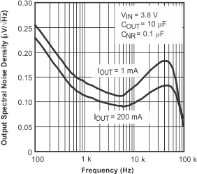
Figure 5-9 TPS793 Output Spectral Noise Density vs Frequency
TPS793 TPS793 Output Spectral Noise Density vs Frequency
COUT = 10uF (new chip)
Figure 5-11 TPS793 Output Spectral Noise Density vs Frequency
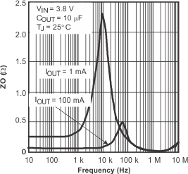
TPS793 Output Impedance vs Frequency
New chip
Figure 5-13 Output Impedance vs Frequency
TPS793 TPS793 Dropout Voltage vs Junction Temperature
New chip
Figure 5-15 TPS793 Dropout Voltage vs Junction Temperature
TPS793 TPS793 Ripple Rejection vs Frequency
Legacy chip
Figure 5-17 TPS793 Ripple Rejection vs Frequency
TPS793 TPS793 Ripple Rejection vs Frequency
New chip
Figure 5-19 TPS793 Ripple Rejection vs Frequency
TPS793 TPS793 Output Voltage, Enable Voltage vs Time (Start-Up)
Legacy chip
Figure 5-21 TPS793 Output Voltage, Enable Voltage vs Time (Start-Up)
TPS793 TPS793 Line Transient Response
Legacy chip
Figure 5-23 TPS793 Line Transient Response
TPS793 TPS79328 Load Transient Response
Legacy chip
Figure 5-25 TPS79328 Load Transient Response
TPS793 Power-Up and Power-Down
Legacy chip
Figure 5-27 Power-Up and Power-Down
TPS793 Dropout Voltage vs Output Current
Legacy chip
Figure 5-29 Dropout Voltage vs Output Current
TPS793 TPS793 Dropout Voltage vs Input Voltage
Legacy chip
Figure 5-31 TPS793 Dropout Voltage vs Input Voltage
TPS793 Typical Regions of Stability Equivalent Series Resistance (ESR) vs Output
                        Current
Legacy chip
Figure 5-33 Typical Regions of Stability Equivalent Series Resistance (ESR) vs Output Current
TPS793 TPS793 Output Voltage vs Output Current
New chip
Figure 5-2 TPS793 Output Voltage vs Output Current
TPS793 TPS793 Output Voltage vs Junction Temperature
New chip
Figure 5-4 TPS793 Output Voltage vs Junction Temperature
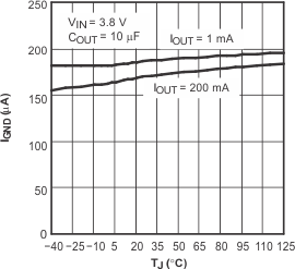
TPS793 TPS793 Ground Current vs Junction Temperature
New chip
Figure 5-6 TPS793 Ground Current vs Junction Temperature
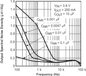
TPS793 TPS793 Output Spectral Noise Density vs Frequency
Legacy chip
Figure 5-8 TPS793 Output Spectral Noise Density vs Frequency
TPS793 Root
                        Mean Square Output Noise vs CNR
Legacy chip
Figure 5-10 Root Mean Square Output Noise vs CNR
TPS793 Output Impedance vs Frequency
Legacy chip
Figure 5-12 Output Impedance vs Frequency
TPS793 TPS793 Dropout Voltage vs Junction Temperature
Legacy chip
Figure 5-14 TPS793 Dropout Voltage vs Junction Temperature
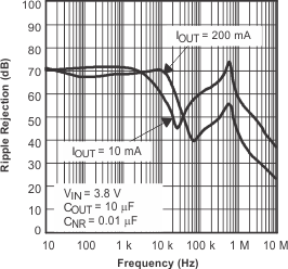
TPS793 TPS793 Ripple Rejection vs Frequency
Legacy chip
Figure 5-16 TPS793 Ripple Rejection vs Frequency
TPS793 TPS793 Ripple Rejection vs Frequency
Legacy chip
Figure 5-18 TPS793 Ripple Rejection vs Frequency
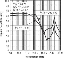
TPS793 TPS793 Ripple Rejection vs Frequency
New chip
Figure 5-20 TPS793 Ripple Rejection vs Frequency
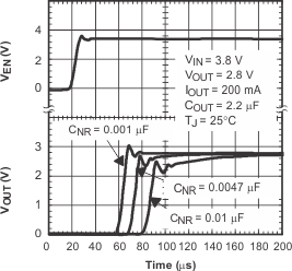
TPS793 TPS793 Output Voltage, Enable Voltage vs Time (Start-Up)
New chip
Figure 5-22 TPS793 Output Voltage, Enable Voltage vs Time (Start-Up)
TPS793 TPS793 Line Transient Response
New chip
Figure 5-24 TPS793 Line Transient Response
TPS793 TPS79328 Load Transient Response
New chip
Figure 5-26 TPS79328 Load Transient Response
TPS793 Power-Up and Power-Down
New chip
Figure 5-28 Power-Up and Power-Down
TPS793 Dropout Voltage vs Output Current
New chip
Figure 5-30 Dropout Voltage vs Output Current
TPS793 TPS793 Dropout Voltage vs Input Voltage
New chip
Figure 5-32 TPS793 Dropout Voltage vs Input Voltage
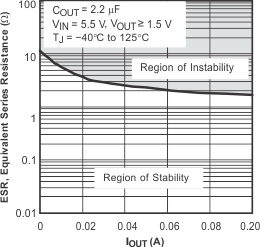
TPS793 Typical Regions of Stability Equivalent Series Resistance (ESR) vs Output
                        Current
Legacy chip
Figure 5-34 Typical Regions of Stability Equivalent Series Resistance (ESR) vs Output Current