SLVS348N July 2001 – January 2025 TPS793
PRODUCTION DATA
- 1
- 1 Features
- 2 Applications
- 3 Description
- 4 Pin Configuration and Functions
- 5 Specifications
- 6 Detailed Description
- 7 Application and Implementation
- 8 Device and Documentation Support
- 9 Revision History
- 10Mechanical, Packaging, and Orderable Information
7.5.1.2 Power Dissipation
The ability to remove heat from the die is different for each package type, presenting different considerations in the printed circuit board (PCB) layout. The PCB area around the device that is free of other components moves the heat from the device to the ambient air. Performance data for JEDEC low- and high-K boards are given in the Thermal Information table. Using heavier copper increases the effectiveness in removing heat from the device. The addition of plated through-holes to heat-dissipating layers also improves the heatsink effectiveness.
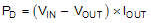
Power dissipation depends on input voltage and load conditions. Power dissipation (PD) can be approximated by the product of the output current times the voltage drop across the output pass element (VIN to VOUT), as shown in Equation 4.
Where:
- TJmax is the maximum allowable junction temperature.
- RθJA is the thermal resistance junction-to-ambient for the package.
- TA is the ambient temperature.
Power dissipation resulting from quiescent current is negligible. Excessive power dissipation triggers the thermal protection circuit.
Figure 7-8 shows the maximum ambient temperature versus the power dissipation of the TPS730. This figure assumes the device is soldered on a JEDEC standard, high-K layout with no airflow over the board. Actual board thermal impedances vary widely. If the application requires high power dissipation, having a thorough understanding of the board temperature and thermal impedances is helpful to verify the TPS730 does not operate above a junction temperature of 125°C.
 Figure 7-8 Maximum Ambient Temperature vs Power Dissipation
Estimating the junction temperature can be done by using the thermal metrics ΨJT and ΨJB, shown in the Thermal Information table. These metrics are a more accurate representation of the heat transfer characteristics of the die and the package than RθJA. The junction temperature can be estimated with Equation 5.

where
- PD is the power dissipation shown by Equation 4.
- TT is the temperature at the center-top of the IC package.
- TB is the PCB temperature measured 1 mm away from the IC package on the PCB surface.
Both TT and TB can be measured on actual application boards using a thermo‐gun (an infrared thermometer).
For more information about measuring TT and TB, see the application note Using New Thermal Metrics (SBVA025), available for download at www.ti.com.