SLVSDR8B April 2018 – February 2023 TPS62147 , TPS62148
PRODUCTION DATA
- 1 Features
- 2 Applications
- 3 Description
- 4 Revision History
- 5 Device Comparison Table
- 6 Pin Configuration and Functions
- 7 Specifications
- 8 Parameter Measurement Information
-
9 Detailed Description
- 9.1 Overview
- 9.2 Functional Block Diagram
- 9.3 Feature Description
- 9.4
Device Functional Modes
- 9.4.1 Pulse Width Modulation (PWM) Operation
- 9.4.2 Power Save Mode Operation (PWM/PFM)
- 9.4.3 100% Duty-Cycle Operation
- 9.4.4 Current Limit And Short Circuit Protection (for TPS62148)
- 9.4.5 HICCUP Current Limit And Short Circuit Protection (for TPS62147)
- 9.4.6 Soft Start / Tracking (SS/TR)
- 9.4.7 Output Discharge Function (TPS62148 only)
- 9.4.8 Starting into a Pre-Biased Load
- 10Application and Implementation
- 11Device and Documentation Support
- 12Mechanical, Packaging, and Orderable Information
9.4.2 Power Save Mode Operation (PWM/PFM)
When the MODE pin is low, Power Save Mode is allowed. The device operates in PWM mode as long the output current is higher than half the inductor ripple current. To maintain high efficiency at light loads, the device enters Power Save Mode at the boundary to discontinuous conduction mode (DCM). This happens if the output current becomes smaller than half the inductor ripple current. For improved transient response, PWM mode is forced for 8 switching cycles if the output voltage is above target due to a load release. The Power Save Mode is entered seamlessly, if the load current decreases and the MODE pin is set low. This ensures a high efficiency in light load operation. The device remains in Power Save Mode as long as the inductor current is discontinuous.
In Power Save Mode the switching frequency decreases linearly with the load current maintaining high efficiency. The transition into and out of Power Save Mode is seamless in both directions.
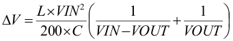
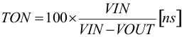
The AEE function in TPS62147, TPS62148 adjusts the on-time (TON) in power save mode depending on the input voltage and the output voltage to maintain highest efficiency. The on-time, in steady-state operation, can be estimated as follows.
For FSEL = high (2.5MHz):
For FSEL = low (1.25MHz):
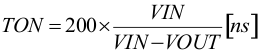
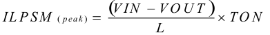
For very small output voltages, an absolute minimum on-time of about 50 ns is kept to limit switching losses. The operating frequency is thereby reduced from its nominal value, which keeps efficiency high. Using TON, the typical peak inductor current in Power Save Mode is approximated by:
There is a minimum off-time which limits the duty cycle of the TPS62147, TPS62148. When VIN decreases to typically 15% above VOUT, the TPS62147, TPS62148 does not enter Power Save Mode, regardless of the load current. The device maintains output regulation in PWM mode.
The output voltage ripple in power save mode is given by Equation 6: