SLVSDR8B April 2018 – February 2023 TPS62147 , TPS62148
PRODUCTION DATA
- 1 Features
- 2 Applications
- 3 Description
- 4 Revision History
- 5 Device Comparison Table
- 6 Pin Configuration and Functions
- 7 Specifications
- 8 Parameter Measurement Information
-
9 Detailed Description
- 9.1 Overview
- 9.2 Functional Block Diagram
- 9.3 Feature Description
- 9.4
Device Functional Modes
- 9.4.1 Pulse Width Modulation (PWM) Operation
- 9.4.2 Power Save Mode Operation (PWM/PFM)
- 9.4.3 100% Duty-Cycle Operation
- 9.4.4 Current Limit And Short Circuit Protection (for TPS62148)
- 9.4.5 HICCUP Current Limit And Short Circuit Protection (for TPS62147)
- 9.4.6 Soft Start / Tracking (SS/TR)
- 9.4.7 Output Discharge Function (TPS62148 only)
- 9.4.8 Starting into a Pre-Biased Load
- 10Application and Implementation
- 11Device and Documentation Support
- 12Mechanical, Packaging, and Orderable Information
3 Description
The TPS62147 and TPS62148 are high efficiency and easy-to-use synchronous step-down DC/DC converters, based on the DCS-Control Topology. The wide input voltage range of 3-V to 17-V make the devices suitable for multi-cell Li-Ion as well as 12-V intermediate supply rails. The devices provide 2-A continuous output current. The devices automatically enter Power Save Mode at light loads to maintain high efficiency across the whole load range. With that, the devices are well suited for applications that require connected standby performance, like industrial PC and video surveillance. With the MODE pin set to low, the switching frequency is adapted automatically based on the output current and also on input and output voltage. This technique is called Automatic Efficiency Enhancement (AEE) and maintains high conversion efficiency over the whole operation range. TPS62147, TPS62148 provide a 1% output voltage accuracy in PWM mode and therefore enable the design of a power supply with high output voltage accuracy. The FSEL pin allows to set a switching frequency in forced PWM mode of 1.25 MHz or 2.5 MHz, respectively.
The typical quiescent current is 18 µA. In shutdown mode, the current is typically 1 µA.
The devices are available as an adjustable version, packaged in a 3-mm × 2-mm VQFN package.
| PART NUMBER(2) | PACKAGE(1) | BODY SIZE (NOM) |
|---|---|---|
| TPS62147 | RGX (VQFN, 11) | 3.00 mm × 2.00 mm |
| TPS62148 | 3.00 mm × 2.00 mm |
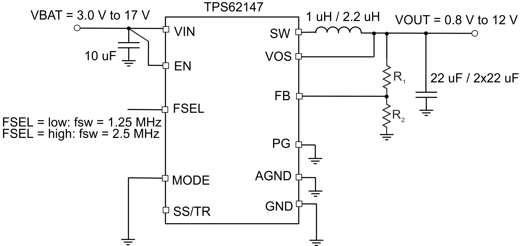
 Simplified Schematic
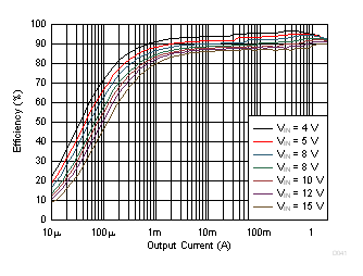
 Efficiency vs Output Current for Vo = 3.3 V;
fsw = 1.25 MHz; PFM