SLVSDR8B April 2018 – February 2023 TPS62147 , TPS62148
PRODUCTION DATA
- 1 Features
- 2 Applications
- 3 Description
- 4 Revision History
- 5 Device Comparison Table
- 6 Pin Configuration and Functions
- 7 Specifications
- 8 Parameter Measurement Information
-
9 Detailed Description
- 9.1 Overview
- 9.2 Functional Block Diagram
- 9.3 Feature Description
- 9.4
Device Functional Modes
- 9.4.1 Pulse Width Modulation (PWM) Operation
- 9.4.2 Power Save Mode Operation (PWM/PFM)
- 9.4.3 100% Duty-Cycle Operation
- 9.4.4 Current Limit And Short Circuit Protection (for TPS62148)
- 9.4.5 HICCUP Current Limit And Short Circuit Protection (for TPS62147)
- 9.4.6 Soft Start / Tracking (SS/TR)
- 9.4.7 Output Discharge Function (TPS62148 only)
- 9.4.8 Starting into a Pre-Biased Load
- 10Application and Implementation
- 11Device and Documentation Support
- 12Mechanical, Packaging, and Orderable Information
10.1.3 Inductor Selection
The TPS62147, TPS62148 are designed for a nominal 1-µH inductor if FSEL = high and a 1.5-uH or 2.2-uH inductor if FSEL = low. Larger values can be used to achieve a lower inductor current ripple but they can have a negative impact on efficiency and transient response. Smaller values than 1 µH cause a larger inductor current ripple which causes larger negative inductor current in forced PWM mode at low or no output current. Therefore they are not recommended at large voltages across the inductor as it is the case for high input voltages and low output voltages. With low output current in forced PWM mode this causes a larger negative inductor current peak which can exceed the negative current limit.
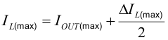
The inductor selection is affected by several effects like inductor ripple current, output ripple voltage, PWM-to-PFM transition point and efficiency. In addition, the inductor selected has to be rated for appropriate saturation current and dc resistance (DCR). Equation 11 calculates the maximum inductor current.
where
- IL(max) is the maximum inductor current
- ΔIL is the Peak to Peak Inductor Ripple Current
- L(min) is the minimum effective inductor value.
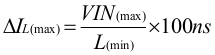
Above equation is valid for FSEL = high. With FSEL = low, the ON-time is doubled from 100 ns to 200 ns so the peak inductor current doubles given the same input voltage and inductor.
Calculating the maximum inductor current using the actual operating conditions gives the minimum saturation current of the inductor needed. A margin of about 20% is recommended to add. A larger inductor value is also useful to get lower ripple current, but increases the transient response time and size as well. The following inductors have been used with the TPS62147, TPS62148 and are recommended for use:
| TYPE | INDUCTANCE [µH] | CURRENT [A](2) | DIMENSIONS [LxBxH] mm | MANUFACTURER(1) |
|---|---|---|---|---|
| XFL3012-102ME | 1.0 µH, ±20% | 2.3 | 3 x 3 x 1.3 | Coilcraft |
| XFL4015-122ME | 1.2µH, ±20% | 4.5 | 4 x 4 x 1.6 | Coilcraft |
| XFL4020-102ME | 1.0 µH, ±20% | 5.4 | 4 × 4 x 2.1 | Coilcraft |
| XFL4020-152ME | 1.5 µH, ±20% | 4.6 | 4 x 4 x 2.1 | Coilcraft |
| XFL4020-222ME | 2.2 µH, ±20% | 3.7 | 4 x 4 x 2.1 | Coilcraft |
| DFE322512F-2R2M | 2.2 µH, ±20% | 2.6 | 3.2 x 2.5 x 1.2 | Murata |
| DFE322512F-1R5M | 1.5 µH, ±20% | 3.0 | 3.2 x 2.5 x 1.2 | Murata |
| DFE322512F-1R0M | 1.0 µH, ±20% | 3.8 | 3.2 x 2.5 x 1.2 | Murata |
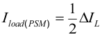
The inductor value also determines the load current at which Power Save Mode is entered: