SLVSDR8B April 2018 – February 2023 TPS62147 , TPS62148
PRODUCTION DATA
- 1 Features
- 2 Applications
- 3 Description
- 4 Revision History
- 5 Device Comparison Table
- 6 Pin Configuration and Functions
- 7 Specifications
- 8 Parameter Measurement Information
-
9 Detailed Description
- 9.1 Overview
- 9.2 Functional Block Diagram
- 9.3 Feature Description
- 9.4
Device Functional Modes
- 9.4.1 Pulse Width Modulation (PWM) Operation
- 9.4.2 Power Save Mode Operation (PWM/PFM)
- 9.4.3 100% Duty-Cycle Operation
- 9.4.4 Current Limit And Short Circuit Protection (for TPS62148)
- 9.4.5 HICCUP Current Limit And Short Circuit Protection (for TPS62147)
- 9.4.6 Soft Start / Tracking (SS/TR)
- 9.4.7 Output Discharge Function (TPS62148 only)
- 9.4.8 Starting into a Pre-Biased Load
- 10Application and Implementation
- 11Device and Documentation Support
- 12Mechanical, Packaging, and Orderable Information
10.3.2 Powering Multiple Loads
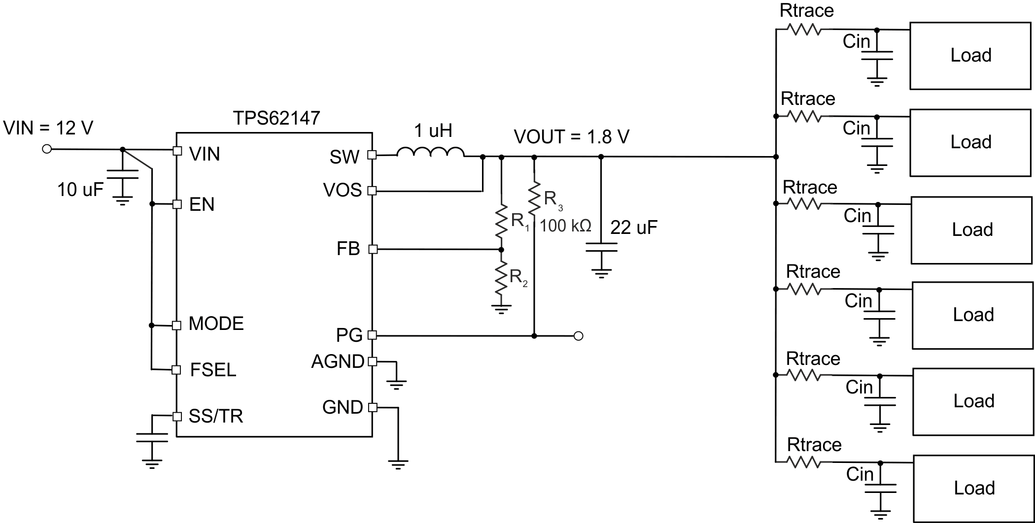
In applications where TPS62147, TPS62148 are used to power multiple load circuits, it can be the case that the total capacitance on the output is very large. To properly regulate the output voltage, there must be an appropriate AC signal level on the VOS pin. Tantalum capacitors have a large enough ESR to keep output voltage ripple sufficiently high on the VOS pin. With low ESR ceramic capacitors, the output voltage ripple can get very low, so it is not recommended to use a large capacitance directly on the output of the device. If there are several load circuits with their associated input capacitor on a pcb, these loads are typically distributed across the board. This adds enough trace resistance (Rtrace) to keep a large enough AC signal on the VOS pin for proper regulation.
The minimum total trace resistance on the distributed load is 10 mΩ. The total capacitance n × Cin in the use case below was 32 × 47 uF of ceramic X7R capacitors.
 Figure 10-81 Multiple Loads