SLVSDR8B April 2018 – February 2023 TPS62147 , TPS62148
PRODUCTION DATA
- 1 Features
- 2 Applications
- 3 Description
- 4 Revision History
- 5 Device Comparison Table
- 6 Pin Configuration and Functions
- 7 Specifications
- 8 Parameter Measurement Information
-
9 Detailed Description
- 9.1 Overview
- 9.2 Functional Block Diagram
- 9.3 Feature Description
- 9.4
Device Functional Modes
- 9.4.1 Pulse Width Modulation (PWM) Operation
- 9.4.2 Power Save Mode Operation (PWM/PFM)
- 9.4.3 100% Duty-Cycle Operation
- 9.4.4 Current Limit And Short Circuit Protection (for TPS62148)
- 9.4.5 HICCUP Current Limit And Short Circuit Protection (for TPS62147)
- 9.4.6 Soft Start / Tracking (SS/TR)
- 9.4.7 Output Discharge Function (TPS62148 only)
- 9.4.8 Starting into a Pre-Biased Load
- 10Application and Implementation
- 11Device and Documentation Support
- 12Mechanical, Packaging, and Orderable Information
10.2.1.2 Detailed Design Procedure
Equation 19. 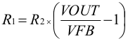
With VFB = 0.7 V:
Table 10-4 Setting the Output Voltage
| NOMINAL OUTPUT VOLTAGE | R1 | R2 | EXACT OUTPUT VOLTAGE |
|---|---|---|---|
| 0.8 V | 51 kΩ | 360 kΩ | 0.799 V |
| 1.2 V | 130 kΩ | 180 kΩ | 1.206 V |
| 1.5 V | 150 kΩ | 130 kΩ | 1.508 V |
| 1.8 V | 470 kΩ | 300 kΩ | 1.797 V |
| 2.5 V | 620 kΩ | 240 kΩ | 2.508 V |
| 3.3 V | 560 kΩ | 150 kΩ | 3.313 V |
| 5 V | 510 kΩ | 82 kΩ | 5.054 V |
| 9 V | 510 kΩ | 43 kΩ | 9.002 V |
| 12 V | 1000 kΩ | 62 kΩ | 11.99 V |