SLVSDR8B April 2018 – February 2023 TPS62147 , TPS62148
PRODUCTION DATA
- 1 Features
- 2 Applications
- 3 Description
- 4 Revision History
- 5 Device Comparison Table
- 6 Pin Configuration and Functions
- 7 Specifications
- 8 Parameter Measurement Information
-
9 Detailed Description
- 9.1 Overview
- 9.2 Functional Block Diagram
- 9.3 Feature Description
- 9.4
Device Functional Modes
- 9.4.1 Pulse Width Modulation (PWM) Operation
- 9.4.2 Power Save Mode Operation (PWM/PFM)
- 9.4.3 100% Duty-Cycle Operation
- 9.4.4 Current Limit And Short Circuit Protection (for TPS62148)
- 9.4.5 HICCUP Current Limit And Short Circuit Protection (for TPS62147)
- 9.4.6 Soft Start / Tracking (SS/TR)
- 9.4.7 Output Discharge Function (TPS62148 only)
- 9.4.8 Starting into a Pre-Biased Load
- 10Application and Implementation
- 11Device and Documentation Support
- 12Mechanical, Packaging, and Orderable Information
10.1.6 Output Filter and Loop Stability
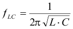
The TPS62147, TPS62148 are internally compensated to be stable with L-C filter combinations corresponding to a corner frequency to be calculated with Equation 16:
Proven nominal values for inductance and ceramic capacitance are given in Table 10-1 and are recommended for use. Different values can work, but care has to be taken for the loop stability which is affected.
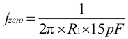
The TPS62147, TPS62148 include an internal 15 pF feedforward capacitor, connected between the VOS and FB pins. This capacitor impacts the frequency behavior and sets a pole and zero in the control loop with the resistors of the feedback divider, per equation Equation 17 and Equation 18:
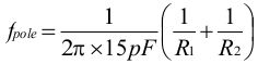
Though the TPS62147, TPS62148 are stable without the pole and zero being in a particular location, adjusting their location to the specific needs of the application can provide better performance in Power Save mode and/or improved transient response. An external feedforward capacitor can also be added. A more detailed discussion on the optimization for stability versus transient response can be found in SLVA289 and SLVA466.