SLWU067D November 2009 – March 2022 ADS4122 , ADS4125 , ADS4126 , ADS4128 , ADS4129 , ADS4142 , ADS4145 , ADS4146 , ADS4149 , ADS41B25 , ADS41B29 , ADS41B49 , ADS58B18 , ADS58B19
2.2.2.2 Clock Option 2
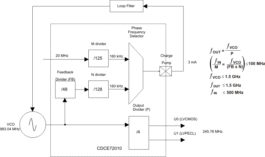
Option 2 uses the onboard VCXO and CDCE72010 to provide a clock to the ADC. The CDCE72010 is used in SPI mode which uses the internal EEPROM to configure the CDCE72010. The EEPROM is programmed in the factory for a divide-by-4 configuration. The EEPROM configuration is shown in Figure 2-4. The clock at J19 is the reference clock for CDCE72010. The VCXO frequency can be calculated as Fvcxo = Fout x 4 (Fout is the frequency output U0 and U1). The reference clock for CDCE72010 is calculated from Ref Clock = (Fvcxo x 125)/(48 x 128). This is the clock-to-M divider. When VCXO of frequency 983.04 MHz is used, the calculation results in a reference clock of 20 MHz; the clock output on Y0 pin of CDCE72010 is 245.76 MHz. This clock is filtered using the crystal filter with center frequency of 245.76 MHz. By default, the VCXO and the crystal filter are not populated on the EVM, so that the user can populate the components depending on the end application and sampling rate. This configuration is recommended for applications requiring an onboard clock generation scheme. The test result using this option is shown in Figure 2-4.
 Figure 2-4 CDCE72010 EEPROM Configuration Block Diagram