SNLA113C november 2008 – june 2023 DS91M124 , DS91M125 , SN65LVDM050 , SN65LVDM050-Q1 , SN65LVDM051 , SN65LVDM051-Q1 , SN65LVDM1676 , SN65LVDM1677 , SN65LVDM176 , SN65LVDM179 , SN65LVDM180 , SN65LVDM22 , SN65LVDM31 , SN65MLVD040 , SN65MLVD047A , SN65MLVD048 , SN65MLVD080 , SN65MLVD082 , SN65MLVD128 , SN65MLVD129 , SN65MLVD2 , SN65MLVD200A , SN65MLVD202A , SN65MLVD204A , SN65MLVD204B , SN65MLVD206B , SN65MLVD3
- 1
- AN-1926 An Introduction to M-LVDS and Clock and Data Distribution Applications
- Trademarks
- 1 Introduction
- 2 M-LVDS Standard Overview
- 3 Driver Characteristics
- 4 Receiver Characteristics
- 5 M-LVDS Portfolio
- 6 M-LVDS Applications
- 7 Clock Distribution in AdvancedTCA Systems
- 8 Clock Distribution in MicroTCA Systems
- 9 M-LVDS as a Short Reach RS-485 Alternative
- 10Signal Distribution with Point-to-Point Links
- 11Wired-OR Implementation
- 12Design Guidelines
- 13Conclusion
- 14References
- 15Revision History
7 Clock Distribution in AdvancedTCA Systems
AdvancedTCA is PCI Industrial Computer Manufacturers Group’s (PICMG) open standard for modular communications systems with capacity of up to 2.5 Tbps. The standard specifies a range of system level design aspects and parameters including mechanical dimensions, power distribution, thermal considerations and data transport.
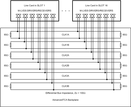
As in many communication systems, AdvancedTCA (ATCA) based systems require synchronization of its internal and external networks. Synchronization Clock Interface is a section of the ATCA Base Specification (PICMG 3.0) that specifies M-LVDS as the signalling technology of choice. In an ATCA system, there are three redundant clocks (totaling 6) distributed to up to 16 backplane slots in a multipoint fashion:
- CLK1A and CLK1B are for redundant 8 kHz standard digital telephony transmission system clocks.
- CLK2A and CLK2B are for 19.44 MHz clocks for synchronization of the SONET/SDH networks.
- CLK3A and CLK3B are for user-defined signals (clock or data).
Each ATCA clock network consists of up to 16 M-LVDS ports connected to a common clock bus as illustrated in Figure 7-1. The clock bus, physically located on the standard backplane, is a 130Ω differential microstrip terminated on both sides with 80Ω resistors. An M-LVDS port is an I/O of a M-LVDS device located on a line card. An interconnect that connects an M-LVDS port to a clock bus is referred to as unterminated stub. A stub in a standard ATCA clock distribution multipoint network consists of a differential trace connecting the M-LVDS device’s I/O pins to the line card’s standard Zone 2 connector pins and the connector’s conductors. The standard ATCA Zone 2 connectors are Advanced Differential Fabric (ADF) connectors such as Tyco’s HM-Zd connectors. Minimizing electrical length of stubs in ATCA clock distribution networks is critical and is discussed later in the design guidelines. The ATCA standard specifies 1 inch (25.4 mm) as the maximum stub length.
 Figure 7-1 AdvancedTCA Clock Distribution
Interface Example