SPRABI1D January 2018 – July 2022 66AK2E05 , 66AK2G12 , 66AK2H06 , 66AK2H12 , 66AK2H14 , 66AK2L06 , AM5K2E02 , AM5K2E04 , SM320C6678-HIREL , TMS320C6652 , TMS320C6654 , TMS320C6655 , TMS320C6657 , TMS320C6670 , TMS320C6671 , TMS320C6672 , TMS320C6674 , TMS320C6678
- Trademarks
- 1 Introduction
- 2 Background
- 3 Migrating Designs From DDR2 to DDR3 (Features and Comparisons)
- 4 Prerequisites
- 5 Package Selection
-
6 Physical Design and Implementation
- 6.1 Electrical Connections
- 6.2 Signal Terminations
- 6.3
Mechanical Layout and Routing Considerations
- 6.3.1
Routing Considerations – SDRAMs
- 6.3.1.1 Mechanical Layout – SDRAMs
- 6.3.1.2 Stack Up – SDRAMs
- 6.3.1.3 Routing Rules – General Overview (SDRAMs)
- 6.3.1.4 Routing Rules – Address and Command Lines (SDRAMs)
- 6.3.1.5 Routing Rules – Control Lines (SDRAMs)
- 6.3.1.6 Routing Rules – Data Lines (SDRAMs)
- 6.3.1.7 Routing Rules – Clock Lines (SDRAMs)
- 6.3.1.8 Routing Rules – Power (SDRAMs)
- 6.3.1.9 Write Leveling Limit Impact on Routing – KeyStone I
- 6.3.1.10 Round-Trip Delay Impact on Routing – KeyStone I
- 6.3.1.11 Write Leveling Limit Impact on Routing – KeyStone II
- 6.3.1.12 Round-Trip Delay Impact on Routing – KeyStone II
- 6.3.2
Routing Considerations – UDIMMs
- 6.3.2.1 Mechanical Layout – UDIMMs
- 6.3.2.2 Stack Up – UDIMMs
- 6.3.2.3 Routing Rules – General Overview (UDIMMs)
- 6.3.2.4 Routing Rules – Address and Command Lines (UDIMMs)
- 6.3.2.5 Routing Rules – Control Lines (UDIMMs)
- 6.3.2.6 Routing Rules – Data Lines (UDIMMs)
- 6.3.2.7 Routing Rules – Clock Lines (UDIMMs)
- 6.3.2.8 Routing Rules – Power (UDIMMs)
- 6.3.2.9 Write-Leveling Limit Impact on Routing
- 6.3.1
Routing Considerations – SDRAMs
- 6.4 Timing Considerations
- 6.5 Impedance Considerations
- 6.6 Switching and Output Considerations
- 7 Simulation and Modeling
- 8 Power
- 9 Disclaimers
- 10References
- 11Revision History
6.3.1.3 Routing Rules – General Overview (SDRAMs)
Several key points to remember when routing any signals on the application board:
- Organize the power, ground, and signal planes so that you eliminate or significantly reduce the number of split or cut planes present in the design (no splits are allowed under any DDR3 routes).
- It is strongly recommended that all SDRAMs are mounted on the top side of the PCB alongside the SoC for single rank designs.
- Apply net classes, for example, group key signals together.
- Maintain an acceptable level of skew across the entire DDR3 interface (by net class).
- Use proper low-pass filtering on the Vref pins.
- Follow the fly-by architecture concept for all address, command, clock, and control lines.
- Increase the size of the decoupling capacitor trace width to as large as possible, keep the stub length as short as possible.
- Center-to-center spacing, including serpentine, must be at least 5 W where W is the trace width. Additional spacing can be added between differential pairs and other routing groups to minimize crosstalk. Spacing of 4 W can be used, but is not appropriate for bus speeds over 1066 MT/s.
- Maintain a common ground reference for all bypass/decoupling capacitors, DSPs, and SDRAMs.
- Take into account the differences in propagation delays between microstrip and stripline nets when evaluating timing constraints. All long routes should be stripline to reduce EMI and timing skew, and any microstrip routed for BGA breakouts should be as short as possible.
- All length-matching is based on an equivalent stripline length. An equivalent stripline length is defined as the length of a stripline trace that will have the same delay as the microstrip portion of the route (see the JEDEC UDIMM specification for more information on velocity compensation).
- There can not be any mid-point vias in the design on any data group net. Extra vias that are located on the data group will negatively impact signal integrity.
- It is strongly recommended that all nets be simulated to assure proper design, performance, and signal integrity.
- Routes along the same path and routing segment must have the same number of vias. Vias can be blind, buried, or HDI microvia for improved SI but are not required for standard data rates. Similarly, back drilling vias is not required for standard data rates but can be used to eliminate via stubs.
- It is strongly recommended that the routing channels between the DSP to SDRAM be dedicated solely to the SDRAM interface and that no other signals be routed in the area. Other signals routed on the same layers must be kept apart from the DDR3 routes. There must be additional separation of the DDR3 nets of at least 6W. In addition, these other traces should not be referenced to the DDR3 IO power planes. If other signals must be routed through this area, they need to be isolated to their own routing planes and shielded from the DDR3 routes by a solid ground plane.
Net classes are an important concept when routing high speed signals that incorporate timing constraints or timing relationships. When routing the DDR3 nets, there are four basic groups (net classes) to consider – Table 6-1 shows the recommended net classes.
| Net Class | Signals |
|---|---|
| Data | DQS[8:0], DQS[8:0], DQ[n:0], CB[7:0], DM[8:0] (1),(2), (4) |
| Address/Command | BA[2:0], A[n:0], RAS, CAS, WE (2), (3) |
| Control | CS, CKE, ODT (2), (5) |
| Clock | DDRCLKOUTP/N[1:0] (5) |
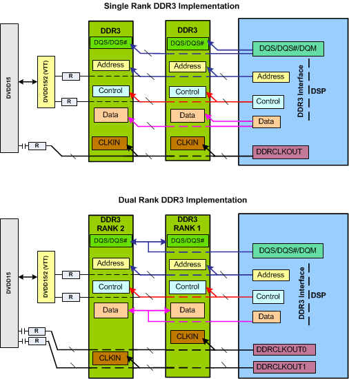
Figure 6-3 shows the typical interface topology when connecting single-rank and dual-rank designs. Note that the dual-rank illustration shows only the connections for byte lane 0, and fly-by connections will still need to include SDRAMs on subsequent byte lanes.
