SPRABN3A May 2022 – June 2022 TMS320F280021 , TMS320F280021-Q1 , TMS320F280023 , TMS320F280023-Q1 , TMS320F280023C , TMS320F280025 , TMS320F280025-Q1 , TMS320F280025C , TMS320F280025C-Q1 , TMS320F280033 , TMS320F280034 , TMS320F280034-Q1 , TMS320F280036-Q1 , TMS320F280036C-Q1 , TMS320F280037 , TMS320F280037-Q1 , TMS320F280037C , TMS320F280037C-Q1 , TMS320F280038-Q1 , TMS320F280038C-Q1 , TMS320F280039 , TMS320F280039-Q1 , TMS320F280039C , TMS320F280039C-Q1 , TMS320F280040-Q1 , TMS320F280040C-Q1 , TMS320F280041 , TMS320F280041-Q1 , TMS320F280041C , TMS320F280041C-Q1 , TMS320F280045 , TMS320F280048-Q1 , TMS320F280048C-Q1 , TMS320F280049 , TMS320F280049-Q1 , TMS320F280049C , TMS320F280049C-Q1 , TMS320F28075 , TMS320F28075-Q1 , TMS320F28076 , TMS320F28374D , TMS320F28374S , TMS320F28375D , TMS320F28375S , TMS320F28375S-Q1 , TMS320F28376D , TMS320F28376S , TMS320F28377D , TMS320F28377D-EP , TMS320F28377D-Q1 , TMS320F28377S , TMS320F28377S-Q1 , TMS320F28378D , TMS320F28378S , TMS320F28379D , TMS320F28379D-Q1 , TMS320F28379S , TMS320F28P550SG , TMS320F28P550SJ , TMS320F28P559SG-Q1 , TMS320F28P559SJ-Q1 , UCD7138
4 Negative Current Detection and Prevention
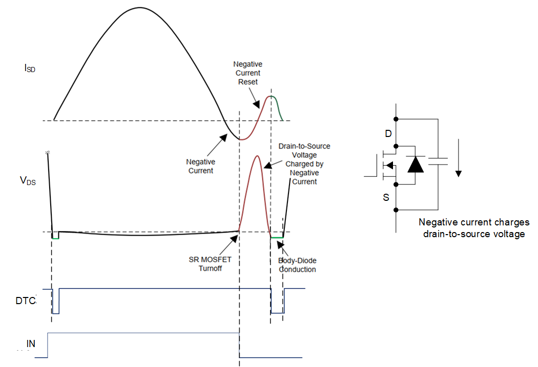
During normal operation, SR control could be always aligned with the primary side PWM signals of LLC converters. However, during large load or line transient operation, the switching frequency of the LLC converter is changed rapidly. Due to the response discrepancy between the primary resonant current and the SR current, it is possible to induce a high risk that SR MOSFETs turn on too long than required, which will cause large negative current and high Vds spikes on SR MOSFETs. As shown in Figure 4-1, the negative current charges up the SR MOSFET drain-to-source capacitance and unexpected Vds overstress might pose a threat to SR MOSFETs when negative current occurs.
 Figure 4-1 SR Drain-to-Source Voltage
Shoot Up
 In the previous art, there is a dedicated interface of UCD3183A controller to handle DTC signal so as to prevent the negative current issue [4]. Within the DTC detection window, shown in Figure 3-1, if no or very-short DTC low time is detected, it means the SR turns off too late. UCD3138A counts the body-diode conduction time of the current cycle and adjusts the SR on time in the next cycle. When the body diode conduction time sensed during the detection window is less than a certain threshold, UCD3138A will treat it as a fault and reduce the SR on time by a large pre-programmed amount.
Though C2000 devices did not provide the DTC interface for UCD7138, the application report discusses how to use CLB to implement the similar negative current prevention scheme with UCD7138. During the normal operations, it is safe to ensure the body diode conducts for a short time, so there will be no DTC high event during the detection window in Figure 3-1, while if turning off the SR too late, DTC will keep high for a while after the falling edge of IN. Thus, it is possible to count the duration of the DTC high time to detect the negative current event.
The below steps show how to leverage CLB module to detect the negative current and prevent it as soon as possible.
- Define the detection window for
the CLB counter, since only the high event between the falling edge of the IN
signal and the rising edge of DTC signal is required to detect. The Finite State
Machine (FSM) block is used to create the detection window, where E0 is referred
to the falling edge of IN, while E1 is the rising edge of DTC, as shown in Figure 4-2. And the FSM equations for S0 can be deduced as Equation 1.
Thus, S0 is used as the “RESET” input for Counter 0, which means the CLB counter will reset to 0 outside the detection window.
Figure 4-2 State Machine in the FSW Block - Then, the original DTC signal is set as the MODE_0 input for the counter, so that the DTC high time can be captured.
- If the captured high-time of DTC is larger than a threshold, a CLB ISR is generated through HLC, indicating the negative current event, and then reduce the SR on time by a large pre-programmed amount for the next cycle. Note that the CLB ISR is suggested to set with highest priority, in order to protect the system with high reliability.
Figure 4-3 shows the completed CLB Tile configuration block diagram, including both resonant tank component compensation scheme in Section 3 and the negative current detection scheme. The CLB ISR is triggered by the Counter 0 MATCH1 event, where MATCH1 is set with the negative detection threshold, like 5, that is 50 ns. Besides, the S0 is also used to trigger HLC to move the counter value of Counter 1 from CLB to CPU at the rising edge of S0, that is also the end of the SR cycle, for the purpose of the SR clamp on-time adjustment.
The below code snippets give an example to show how to handle the negative event in the CLB ISR, where negative_current_flag is used to indicate the SR PWM register will change temporally due to the negative current event, and need to recover to the expected one later.
__interrupt void clb1ISR(void)
{

    negative_current_flag = 1;

EPWM2_CMPA = EPWM2_CMPA-reduce_step;
}