SPRABN3A May 2022 – June 2022 TMS320F280021 , TMS320F280021-Q1 , TMS320F280023 , TMS320F280023-Q1 , TMS320F280023C , TMS320F280025 , TMS320F280025-Q1 , TMS320F280025C , TMS320F280025C-Q1 , TMS320F280033 , TMS320F280034 , TMS320F280034-Q1 , TMS320F280036-Q1 , TMS320F280036C-Q1 , TMS320F280037 , TMS320F280037-Q1 , TMS320F280037C , TMS320F280037C-Q1 , TMS320F280038-Q1 , TMS320F280038C-Q1 , TMS320F280039 , TMS320F280039-Q1 , TMS320F280039C , TMS320F280039C-Q1 , TMS320F280040-Q1 , TMS320F280040C-Q1 , TMS320F280041 , TMS320F280041-Q1 , TMS320F280041C , TMS320F280041C-Q1 , TMS320F280045 , TMS320F280048-Q1 , TMS320F280048C-Q1 , TMS320F280049 , TMS320F280049-Q1 , TMS320F280049C , TMS320F280049C-Q1 , TMS320F28075 , TMS320F28075-Q1 , TMS320F28076 , TMS320F28374D , TMS320F28374S , TMS320F28375D , TMS320F28375S , TMS320F28375S-Q1 , TMS320F28376D , TMS320F28376S , TMS320F28377D , TMS320F28377D-EP , TMS320F28377D-Q1 , TMS320F28377S , TMS320F28377S-Q1 , TMS320F28378D , TMS320F28378S , TMS320F28379D , TMS320F28379D-Q1 , TMS320F28379S , TMS320F28P550SG , TMS320F28P550SJ , TMS320F28P559SG-Q1 , TMS320F28P559SJ-Q1 , UCD7138
2 SR Turn-On Edge Optimization
Figure 2-1 shows the system diagram for C2000 and UCD7138. Normally, digital control scheme will make the SR turn-on edge aligned with the primary side PWM, and further add the rising edge delay to the SR PWM signals. However, a fixed or larger than required rising edge delay could not provide optimal efficiency, due to longer body diode conduction time. Actually, using UCD7138 could optimize the turn-on edge essentially, with CTRL pin floating or connected to logic high (3.3 V).
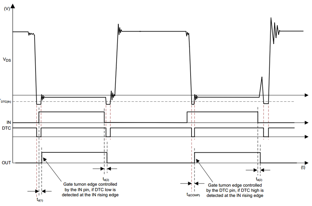
Figure 2-2 shows the turn-on edge optimization scheme with UCD7138. IN is the gate-driver input-command signal from the digital controller, like C2000, and OUT is the SR-gate driver output signal. The DTC pin is the body-diode conduction detector output, and when the body diode of SR MOSFETs conducts, the DTC pin is low.
The actual gate turn-on timing is controlled by both the digital controller output IN and DTC. The OUT can only be turned on when IN is high. If DTC is already low at IN rising edge, turn on the gate driver output immediately; if DTC is still high at IN rising edge, turn on the gate driver output as soon as the DTC falling edge is received. While, the gate turn-off edge is determined by IN only. The gate is turned off immediately at the IN falling edge.
Thus, to make sure the turn-on edge to optimize freely, users could simply set the same rising edge for IN as the primary side PWM with C2000.
 Figure 2-2 Turn-On Edge
Optimization