SPRUJ12F August 2021 – January 2024 AM2431 , AM2432 , AM2434
- 1
- Abstract
- Trademarks
- 1Preface: Read This First
- 2Kit Overview
- 3Board Setup
-
4Hardware Description
- 4.1 Functional Block Diagram
- 4.2 BoosterPack Headers
- 4.3 GPIO Mapping
- 4.4 Reset
- 4.5 Clock
- 4.6 Memory Interface
- 4.7 Ethernet Interface
- 4.8 USB 2.0 Interface
- 4.9 I2C Interface
- 4.10 Industrial Application LEDs
- 4.11 UART Interface
- 4.12 eQEP Interface
- 4.13 CAN Interface
- 4.14 FSI Interface
- 4.15 JTAG Emulation
- 4.16 Test Automation Interface
- 4.17 SPI Interface
- 5References
- A E3 Design Changes
- B Revision A Design Changes
- Revision History
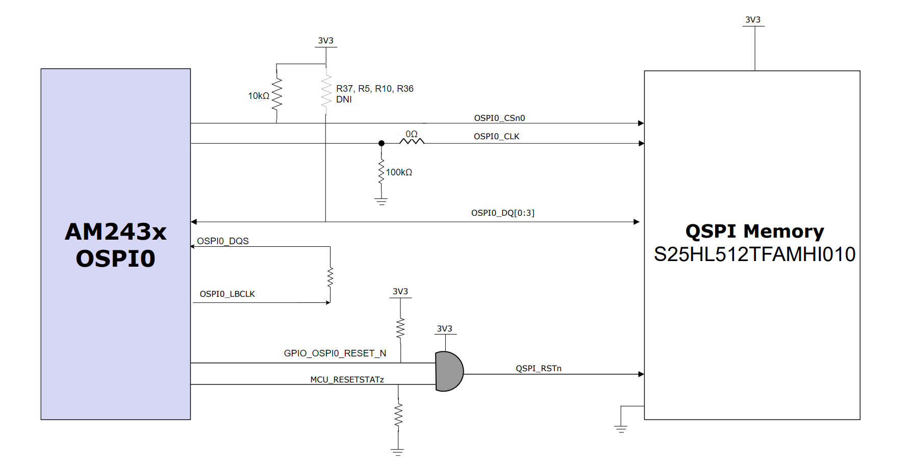
4.6.1 QSPI Interface
The AM243x LaunchPad board has 512 Mbit QSPI memory device (S25HL512TFAMHI010 from Cypress), which is connected to the OSPI0 interface of the AM243x SoC. The QSPI interface supports memory speed up to 166 MHz. External loopback is provided between OSPI0_LBCLKO and OSPI0_DQS.
Reset: The reset for the flash is connected to a circuit that performs an AND operation to MCU_RESETSTATz and a GPIO from the SoC.
Power: The QSPI flash is powered by the 3.3 V IO supply. The 3.3 V supply is provided to both the VCC and VCCQ pins of the flash memory. The OSPI0 interface of the SoC is powered by the VDDSHV_3V3 supply.
 Figure 4-7 QSPI Interface