SPRUJ12F August 2021 – January 2024 AM2431 , AM2432 , AM2434
- 1
- Abstract
- Trademarks
- 1Preface: Read This First
- 2Kit Overview
- 3Board Setup
-
4Hardware Description
- 4.1 Functional Block Diagram
- 4.2 BoosterPack Headers
- 4.3 GPIO Mapping
- 4.4 Reset
- 4.5 Clock
- 4.6 Memory Interface
- 4.7 Ethernet Interface
- 4.8 USB 2.0 Interface
- 4.9 I2C Interface
- 4.10 Industrial Application LEDs
- 4.11 UART Interface
- 4.12 eQEP Interface
- 4.13 CAN Interface
- 4.14 FSI Interface
- 4.15 JTAG Emulation
- 4.16 Test Automation Interface
- 4.17 SPI Interface
- 5References
- A E3 Design Changes
- B Revision A Design Changes
- Revision History
4.11 UART Interface
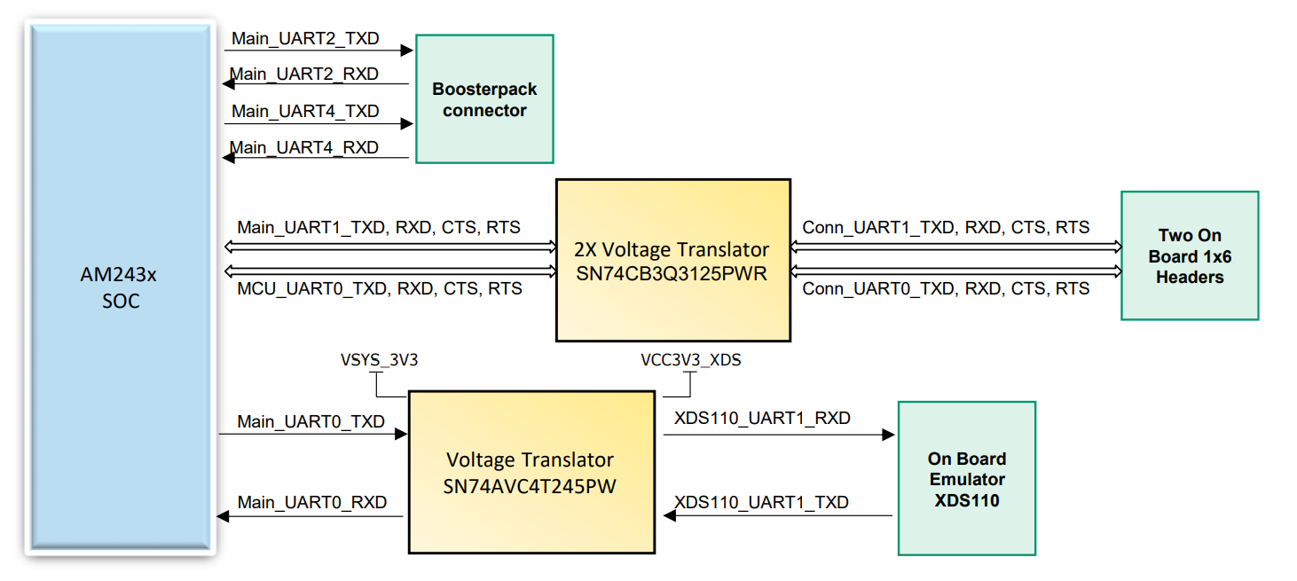
The LaunchPad consists of five UART interfaces where four of the interfaces come from the main domain of the SoC and one comes from the MCU domain.
- Two UART ports from the main domain of the SoC (Main_UART2 and Main_UART4) are terminated on the BoosterPack expansion connectors.
- Two UART, one from the MCU domain (MCU_UART0) and one from the main domain of the SoC (MAIN_UART1) are terminated on two on-board 1x6 headers. There is a buffer (SN74CB3Q3125PWR) used to isolate between the connectors and the SoC.
- One UART port from the main domain of the SoC (Main_UART0) is connected to a buffer (SN74AVC4T245PW) isolated between the SoC and the on-board emulator XDS110 (TM4C1294NCPDTT3R)
 Figure 4-16 UART Interface