SPRUJ12F August 2021 – January 2024 AM2431 , AM2432 , AM2434
- 1
- Abstract
- Trademarks
- 1Preface: Read This First
- 2Kit Overview
- 3Board Setup
-
4Hardware Description
- 4.1 Functional Block Diagram
- 4.2 BoosterPack Headers
- 4.3 GPIO Mapping
- 4.4 Reset
- 4.5 Clock
- 4.6 Memory Interface
- 4.7 Ethernet Interface
- 4.8 USB 2.0 Interface
- 4.9 I2C Interface
- 4.10 Industrial Application LEDs
- 4.11 UART Interface
- 4.12 eQEP Interface
- 4.13 CAN Interface
- 4.14 FSI Interface
- 4.15 JTAG Emulation
- 4.16 Test Automation Interface
- 4.17 SPI Interface
- 5References
- A E3 Design Changes
- B Revision A Design Changes
- Revision History
4.5 Clock
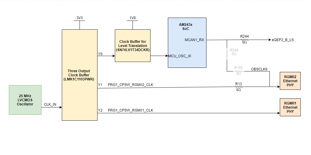
All reference clocks required for the SoC and two Ethernet PHY's are generated from a single three-output clock buffer (LMK1C1103PWR), which is sourced from a single 25 MHz LVCMOS Oscillator. A single output clock buffer (SN74LV1TT34DCKR) is used to level translate from 3.3 V to 1.8 V. An optional clock is provided to RGMII2 Ethernet PHY by the OBSCLK0 output of the SoC by mounting R240 and R185 while isolating R244 and R13.
The reference clock required for XDS110 is generated locally using a 16 MHz crystal.
 Figure 4-6 Clock Architecture
Table 4-16 Clock Frequency Table
| SI # | Signal Name | Reference | Expected Frequency |
|---|---|---|---|
| 1 | SOC_CLKIN | U11.4 | 25.000 MHz |
| 2 | SOC_CLKIN_BUFF | R46 | 25.000 MHz |
| 3 | PRG1_CPSW_RGMII1_CLK | R25 | 25.000 MHz |
| 4 | PRG1_CPSW_RGMII2_CLK | R50 | 25.000 MHz |
| 5 | OSC0 | Y1.3 | 16.000 MHz |
Note: The 16 MHz clock will only become
active after power is supplied to the micro-B USB connector after insertion of a
cable into the micro-B USB port.