SPRUJ12F August 2021 – January 2024 AM2431 , AM2432 , AM2434
- 1
- Abstract
- Trademarks
- 1Preface: Read This First
- 2Kit Overview
- 3Board Setup
-
4Hardware Description
- 4.1 Functional Block Diagram
- 4.2 BoosterPack Headers
- 4.3 GPIO Mapping
- 4.4 Reset
- 4.5 Clock
- 4.6 Memory Interface
- 4.7 Ethernet Interface
- 4.8 USB 2.0 Interface
- 4.9 I2C Interface
- 4.10 Industrial Application LEDs
- 4.11 UART Interface
- 4.12 eQEP Interface
- 4.13 CAN Interface
- 4.14 FSI Interface
- 4.15 JTAG Emulation
- 4.16 Test Automation Interface
- 4.17 SPI Interface
- 5References
- A E3 Design Changes
- B Revision A Design Changes
- Revision History
4.7.1 Ethernet PHY Strapping
The DP83869 uses many of the functional pins as strap options to place the device into specific modes of operation. The values of these pins are sampled at power up or hard reset. During software resets, the strap options are internally reloaded from the values sampled at power up or hard reset. RX_D0 and RX_D1 pins are 4-level strap pins and all other strap pins have two levels.
The Ethernet PHY includes an internal pull-down resistor. The value for the external pull resistors are selected to provide voltage at the pins of the AM243x as close to ground or 3.3 V as possible.
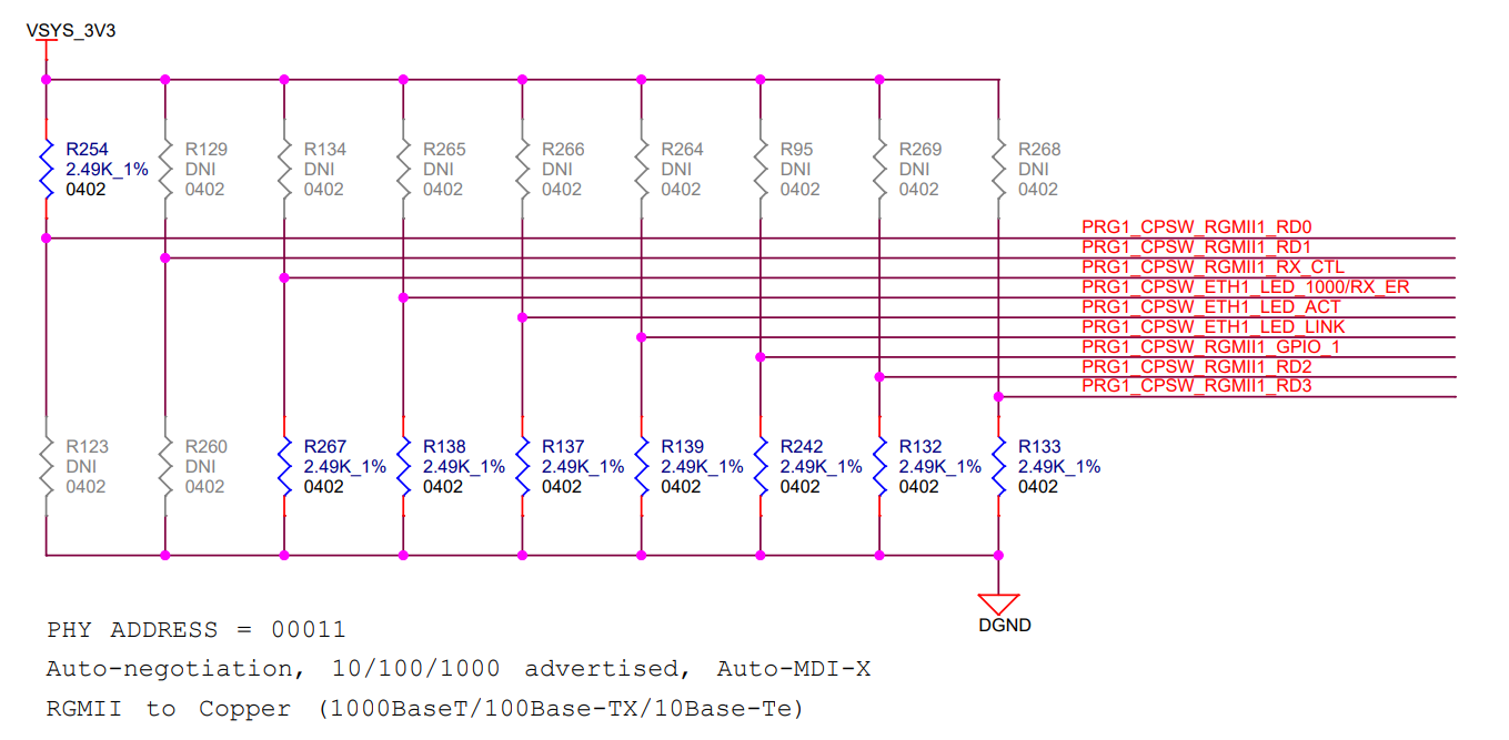
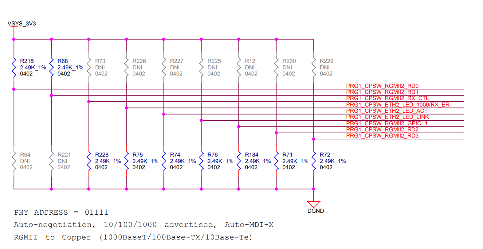
Address strapping is provided for the RGMII1 PHY and RGMII2 PHY to set the address to 00011 (03h) and 0111 (0Fh), respectively, using strap resistors. Footprint for both pull up and pull down is provided on all the strapping pins.
Both PHY modes are selected as RGMII to copper with auto-negotiation advertised for 1000 Base-T, 100 Base-Tx, and 10 Base-Te speeds.
The strapping configurations for both Ethernet PHYs are shown in Figure 4-11 and Figure 4-12.
 Figure 4-11 Ethernet PHY Strapping for
RGMII1 PHY
 Figure 4-12 Ethernet PHY Strapping for
RGMII2 PHY
Figure 4-12 Ethernet PHY Strapping for
RGMII2 PHYTable 4-18 shows the strapping description for both Ethernet PHYs.
| Strap Setting | Pin Name | Strap Function | Value of Strap Function for RGMII1 | Value of Strap Function for RGMII2 | Description |
|---|---|---|---|---|---|
| PHY Address | RX_D1 | PHY_AD3 | 1 | 1 | ICSSG1 PHY Address 00011 |
| PHY_AD2 | 1 | 1 | |||
| RX_D0 | PHY_AD1 | 0 | 1 | ICSSG2PHY Address: 01111 | |
| PHY_AD0 | 0 | 0 | |||
| Modes of Operation | RX_CNTL | Mirror Enable | 0 | 0 | Mirror Enabled/Disabled |
| LED_2 | ANEGSEL_1 | 0 | 0 | Auto-negotiation, 10/100/1000 advertissed, Auto-MDI-X | |
| LED_1 | ANEGSEL_0 | 0 | 0 | ||
| LED_0 | ANEG_DIS | 0 | 0 | ||
| JTAG_TDO/GPIO_1 | OPMODE_0 | 0 | 0 | RGMII to Copper (1000 Base-T, 100 Base-Tx, 10 Base-Te) | |
| RX_D2 | OPMODE_1 | 0 | 0 | ||
| RX_D3 | OPMODE_2 | 0 | 0 |