SPRUJ12F August 2021 – January 2024 AM2431 , AM2432 , AM2434
- 1
- Abstract
- Trademarks
- 1Preface: Read This First
- 2Kit Overview
- 3Board Setup
-
4Hardware Description
- 4.1 Functional Block Diagram
- 4.2 BoosterPack Headers
- 4.3 GPIO Mapping
- 4.4 Reset
- 4.5 Clock
- 4.6 Memory Interface
- 4.7 Ethernet Interface
- 4.8 USB 2.0 Interface
- 4.9 I2C Interface
- 4.10 Industrial Application LEDs
- 4.11 UART Interface
- 4.12 eQEP Interface
- 4.13 CAN Interface
- 4.14 FSI Interface
- 4.15 JTAG Emulation
- 4.16 Test Automation Interface
- 4.17 SPI Interface
- 5References
- A E3 Design Changes
- B Revision A Design Changes
- Revision History
4.2 BoosterPack Headers
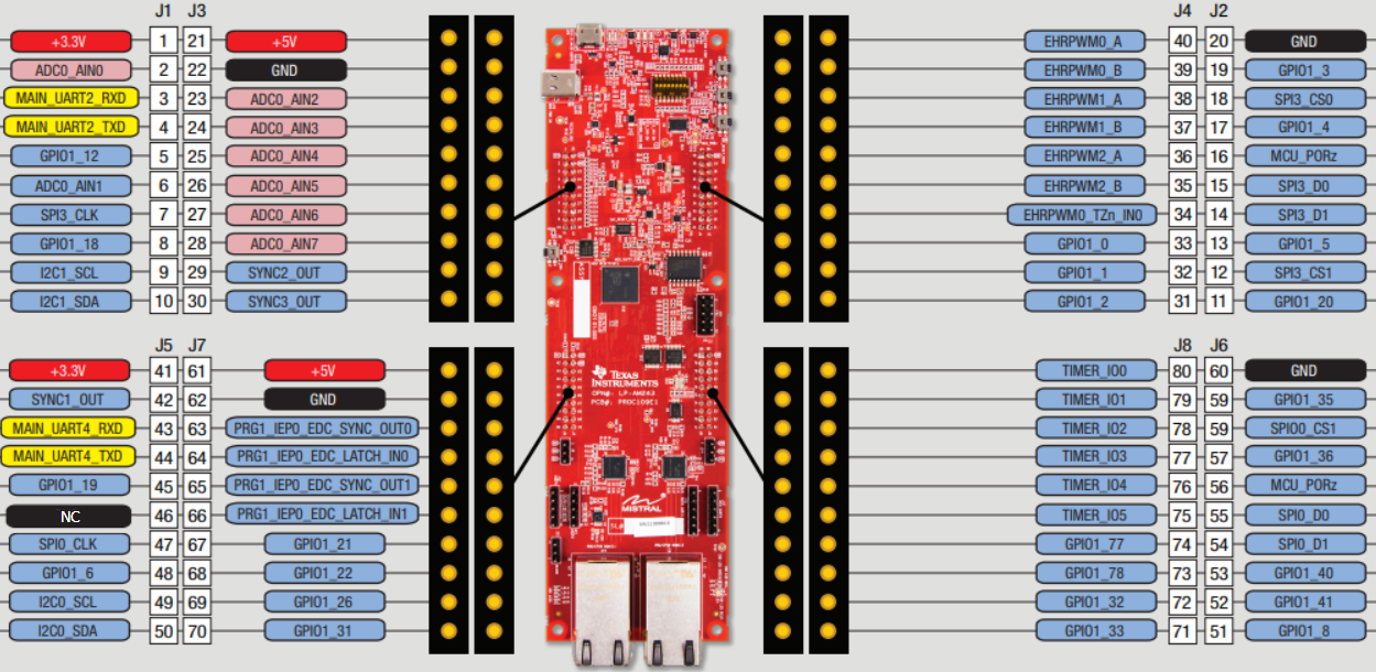
 Figure 4-2 BoosterPack Header
Pinout
Figure 4-2 BoosterPack Header
PinoutThe AM243x LaunchPad supports two fully independent BoosterPack XL connectors. BoosterPack site #1 (J1/J3, J2/J4) is located in between the SoC and the bootmode DIP switch. BoosterPack site #2 (J5/J7, J6/J8) is located in between the SoC and the RJ45 connectors. The GPIO pin numbers as well as the BoosterPack compliant features are listed in Figure 4-2. Each GPIO has multiple functions available through the GPIO mux. The signals connected from the SoC to the BoosterPack headers include:
- SPI0 and SPI3
- UART0 and UART2
- I2C0 and I2C1
- MMC1
- ADC0
- EHRPWM0_A/B and EHRPWM1_A/B
- GPIO's
- 5 V and 3.3 V power supplies
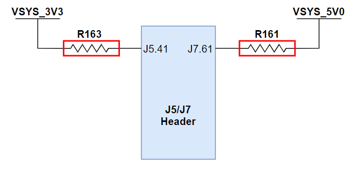
A BoosterPack that is connected to site #1 will be powered by the AM243x. A BoosterPack that is connected to site #2 can either be powered by the AM243x or have it's power sourced from the Boosterpack itself depending on whether or not the 0Ω resistors (R161, R163) are mounted. The resistors are mounted by default as shown in Figure 4-3, the AM243x will provide the VSYS_3V3 and VSYS_5V0 source voltage for the BoosterPack. When left unpopulated, the BoosterPack will be required to source its own power.
| Function | Mount R161 and R163 (Default) | Unmount R161 and R163 |
|---|---|---|
| Power to BoosterPack sourced from LaunchPad | ✔ | |
| Power to BoosterPack sourced from the BoosterPack | ✔ |
 Figure 4-3 Site #2 BoosterPack
Header