SWRA726 March 2022 CC1120 , CC1121 , CC1201 , CC1310 , CC1311P3 , CC1311R3 , CC1312PSIP , CC1312R , CC1312R7 , CC1314R10 , CC1350 , CC1352P , CC1352R , CC1354P10 , CC1354R10 , CC2340R5-Q1 , CC2640R2L , CC2651R3 , CC2652P , CC2652P7 , CC2652R , CC2652R7 , CC2652RB , CC2652RSIP , CC3130 , CC3135MOD , CC3230S , CC3235MODAS , CC3235MODASF , CC3235MODSF , CC3235S , WL1801MOD , WL1805MOD , WL1807MOD , WL1831 , WL1831MOD , WL1835MOD , WL1837MOD
- Trademarks
- 1Introduction
- 2Antenna Standing Wave Ratio (SWR) Measurement
- 3Evaluation Board Matching Components Location
- 4Volpert-Smith Chart
- 5868-MHz PCB Helix Antenna Measurement and Matching
- 62.4-GHz PCB Compact Antenna Measurement and Matching
- 7 2.4-GHz PCB Inverted-F Antenna Measurement and Matching
- 8Fast in-circuit or in-device Antenna Verification
- 9Conclusion
4.3 VNA Calibration Procedure
Calibration method described below can’t be high precise as it’s impossible to make a precision short, open and matched loads on the board, especially for frequencies above 2 GHz due to parasitic elements (short load will always have an inductance and open load a fringing capacitance), but reasonably sufficient for antenna in-device measurement and matching.
An example of typical Pi-matching network (not in scale) and DC blocking capacitor on PCB are shown on Figure 4-15.
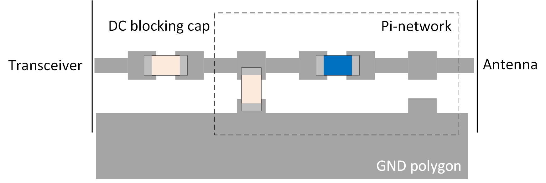 Figure 4-15 Typical Matching Network
Matching components should be removed (if not already) from the board and matching network isolated from a transceiver (for example, removed DC blocking capacitor). An example with connected semi-rigid cable and SOL calibration point is shown on Figure 4-16.
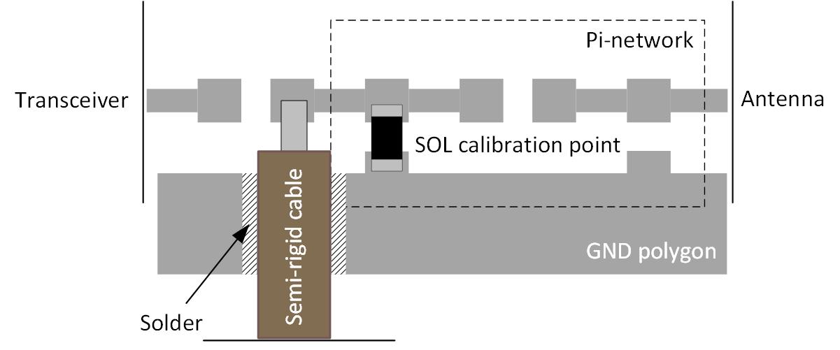 Figure 4-16 Example of Semi-Rigid Coaxial Cable Connection to Matching Network
- For
calibration “Open” load - solder the shield to main PCB ground plane close to
antenna’s feed point and leave an inner conductor unconnected (Figure 4-17).
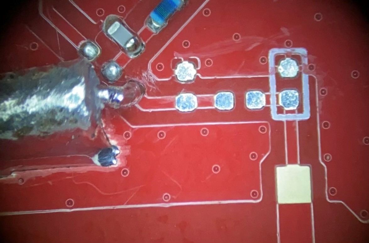 Figure 4-17 VNA Calibration for
Open Load
 - For calibration “Short” load -
solder the inner conductor to the shield. In this example SMD jumper of 0 Ohm
was used (Figure 4-18).
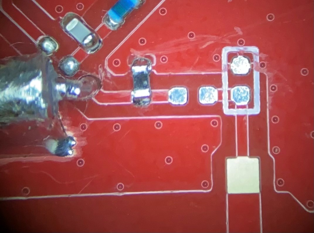 Figure 4-18 VNA Calibration for
Short Load
 - For calibration matched 50 Ohm
“Load” – two shunt SMD resistors of 100 Ohm each (or one of 49.9 Ohm or 50 Ohm)
can be used. The resistors should be soldered to the inner conductor and shield
(Figure 4-19).
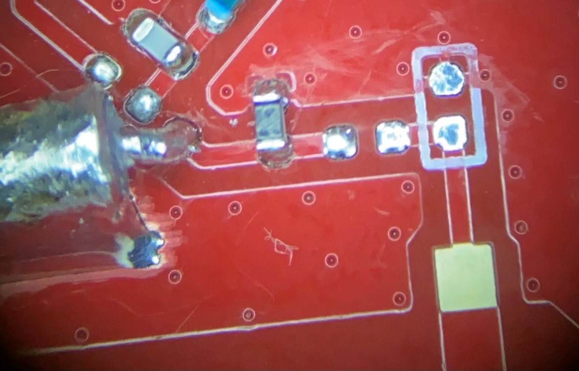 Figure 4-19 VNA Calibration for
Matched 50-Ohm Load
Depending on what VNA model users use, an option for delay can have different menu name (for example, port extension). Port extension allows users to move electrically a measurement reference plane after the calibration.
Figure 4-20 shows uncompensated delay after the calibration with short load connected at 868 MHz frequency. So, the VNA is showing connected short load as not the short load. If the compensation will not be done, it can compromise measured impedance value of the antenna, so the final matching of the antenna will be incorrect and far in comparison with a real antenna’s behavior.
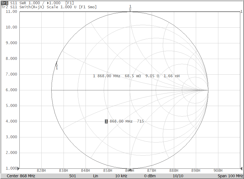 Figure 4-20 Uncompensated Delay with
Short-Load Connected
Figure 4-20 Uncompensated Delay with
Short-Load ConnectedAfter the compensation, the marker should indicate the Short load. Compensated delay of 32.82 ps is shown on Figure 4-21.
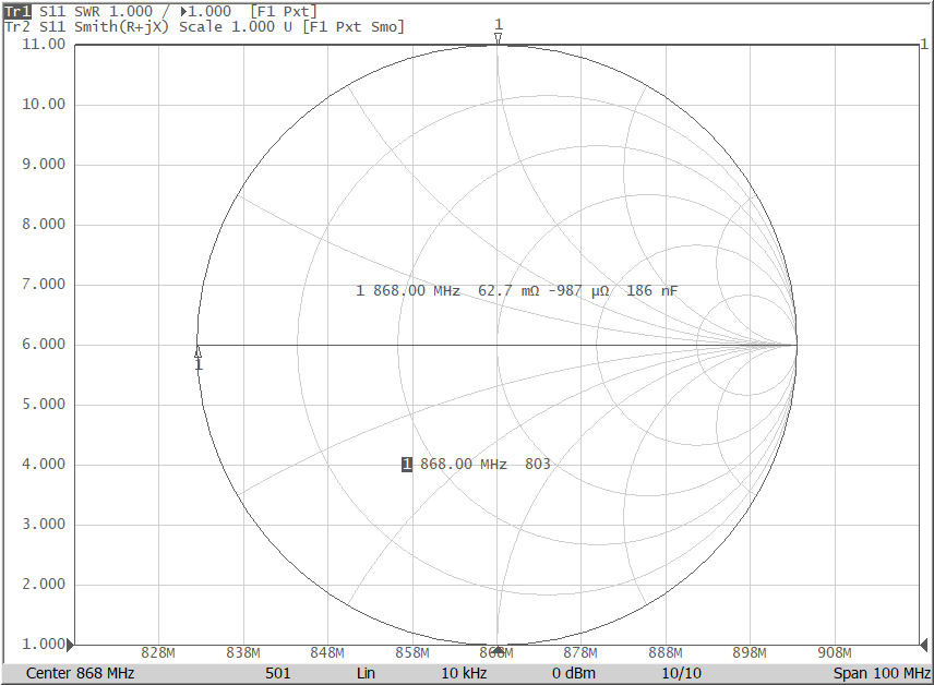 Figure 4-21 Compensated Delay with
Short-Load Connected
Figure 4-21 Compensated Delay with
Short-Load ConnectedCompensation (port extension) can be done with open load as well. The short load just better as gives higher level of reflections to VNA port. In reality, short and open loads have slightly different delays even for the precision calibration kits.
It is good practice to measure losses (skin effect losses) and compensate them if VNA supports this feature.