TIDUDS9B December 2017 – November 2022
- Description
- Resources
- Features
- Applications
- 5
- 1System Description
-
2System Overview
- 2.1 Block Diagram
- 2.2
Design Considerations
- 2.2.1 Conditions of Use: Assumption
- 2.2.2
Diagnostics Coverage
- 2.2.2.1 Dual-Channel Monitoring
- 2.2.2.2 Checking ISO1211 Functionality With MCU (SIL1)
- 2.2.2.3 Checking TPS22919 Functionality With MCU (SIL1)
- 2.2.2.4 Checking TPS27S100 Functionality With MCU (SIL1)
- 2.2.2.5 Optional Monitoring Using RDY Pin of ISO5452, ISO5852S or UCC21750 Integrated Analog-to-PWM Isolated Sensor
- 2.2.3 Drive State
- 2.3 Highlighted Products
- 2.4 System Design Theory
-
3Hardware, Software, Testing Requirements, and Test Results
- 3.1 Getting Started Hardware
- 3.2 Testing and Results
- 4Design Files
- 5Related Documentation
- 6About the Author
- 7Recognition
- 8Revision History
2.4.3.1 High-Side Switch for Controlling Secondary-Side Supply Voltage of Gate Driver
The TPS27S100x is a single-channel, fully-protected, high-side switch with an integrated NMOS and charge pump. An external adjustable current limit improves the reliability of the whole system by clamping the inrush or overload current. Figure 2-12 shows the schematic design of the TPS27S100.
 Figure 2-12 TPS27S100 Schematic
The device power supply is 24-V which is assumed to be protected against fault and remains within ±20% tolerance. Pin 3 Enable the control for channel activation by signal STO2_EN.
Equation 6 calculates the value of resistor R4, which is required to keep the 1-A nominal current in the 0- to 3.3-V current-sense range. To achieve better current-sense accuracy, a 1% tolerance or better resistor is preferred.
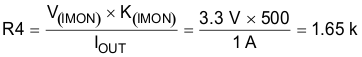
The value of resistor R4 is selected as 1.65 K. The current-sense (CS) pin is connected to the ADC input of the diagnostic MCU (SIL 1) with a low-pass filter (R3 and C6).
To set the adjustable current limit value at 1 A, calculate R7 using Equation 7.
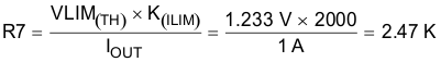
The value of resistor R7 is selected as 2.55 kΩ.
The enable pin is permanently connected to 3.3 V to enable continuous diagnostic monitoring and also send back to the diagnostic MCU (SIL 1).