TIDUDS9B December   2017  – November 2022


  1.   Description
  2.   Resources
  3.   Features
  4.   Applications
  5.   5
  6. 1System Description
    1. 1.1 Key System Specifications
  7. 2System Overview
    1. 2.1 Block Diagram
    2. 2.2 Design Considerations
      1. 2.2.1 Conditions of Use: Assumption
        1. 2.2.1.1 Generic Assumptions
        2. 2.2.1.2 Specific Assumptions
      2. 2.2.2 Diagnostics Coverage
        1. 2.2.2.1 Dual-Channel Monitoring
        2. 2.2.2.2 Checking ISO1211 Functionality With MCU (SIL1)
        3. 2.2.2.3 Checking TPS22919 Functionality With MCU (SIL1)
        4. 2.2.2.4 Checking TPS27S100 Functionality With MCU (SIL1)
        5. 2.2.2.5 Optional Monitoring Using RDY Pin of ISO5452, ISO5852S or UCC21750 Integrated Analog-to-PWM Isolated Sensor
      3. 2.2.3 Drive State
    3. 2.3 Highlighted Products
      1. 2.3.1 ISO1211
      2. 2.3.2 TPS27S100
      3. 2.3.3 TPS22919
      4. 2.3.4 ISO5852S, ISO5452
    4. 2.4 System Design Theory
      1. 2.4.1 Digital Input Receiver for STO
      2. 2.4.2 STO_1 Signal Flow Path for Controlling VCC1
      3. 2.4.3 STO_2 Signal Flow Path
        1. 2.4.3.1 High-Side Switch for Controlling Secondary-Side Supply Voltage of Gate Driver
        2. 2.4.3.2 Powering up Secondary Side: VCC2 of Gate Driver
      4. 2.4.4 Gate Driver Design
      5. 2.4.5 STO_FB Signal Flow Path
  8. 3Hardware, Software, Testing Requirements, and Test Results
    1. 3.1 Getting Started Hardware
      1. 3.1.1 PCB Overview
    2. 3.2 Testing and Results
      1. 3.2.1 Logic High and Logic Low STO Thresholds
      2. 3.2.2 Validation of STO1 Signal
        1. 3.2.2.1 Propagation of STO1 to VCC1 of Gate Driver
        2. 3.2.2.2 1-ms STO Pulse Rejection
        3. 3.2.2.3 Diagnostic Pulses From MCU Interface
      3. 3.2.3 Validation of STO2 Signals
        1. 3.2.3.1 Propagation of STO2 to VCC2 of Gate Driver
        2. 3.2.3.2 1-ms Pulse Rejection
        3. 3.2.3.3 Diagnostic Pulses From MCU
        4. 3.2.3.4 Inrush Current Measurement
      4. 3.2.4 3.3-V Voltage Rail From Switcher
      5. 3.2.5 60-V Input Voltage and Reverse Polarity Protection
      6. 3.2.6 Validation of Trip Zone Functionality
  9. 4Design Files
    1. 4.1 Schematics
    2. 4.2 Bill of Materials
    3. 4.3 Layer Plots
    4. 4.4 Altium Project
    5. 4.5 Gerber Files
    6. 4.6 Assembly Drawings
  10. 5Related Documentation
    1. 5.1 Trademarks
  11. 6About the Author
  12. 7Recognition
  13. 8Revision History

ISO1211

Figure 2-6 shows the pin diagram of the ISO1211. The ISO1211 devices are isolated, 24- to 60-V digital input receivers These receivers are compliant to IEC 61131-2 Type 1, 2, and 3 characteristics and suitable for programmable logic Controllers (PLCs) and motor-control digital input modules. Unlike traditional optocoupler solutions with discount, impair current-limiting circuit, the ISO121x devices provide a simple, low-power solution with an accurate current limit to enable the design of compact and high-density I/O modules. These devices do not require field-side power.
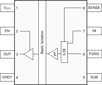
GUID-849BC0FE-8E18-452B-B108-B0345F281F13-low.gifFigure 2-6 ISO1211 Pin Diagram