TIDUDS9B December 2017 – November 2022
- Description
- Resources
- Features
- Applications
- 5
- 1System Description
-
2System Overview
- 2.1 Block Diagram
- 2.2
Design Considerations
- 2.2.1 Conditions of Use: Assumption
- 2.2.2
Diagnostics Coverage
- 2.2.2.1 Dual-Channel Monitoring
- 2.2.2.2 Checking ISO1211 Functionality With MCU (SIL1)
- 2.2.2.3 Checking TPS22919 Functionality With MCU (SIL1)
- 2.2.2.4 Checking TPS27S100 Functionality With MCU (SIL1)
- 2.2.2.5 Optional Monitoring Using RDY Pin of ISO5452, ISO5852S or UCC21750 Integrated Analog-to-PWM Isolated Sensor
- 2.2.3 Drive State
- 2.3 Highlighted Products
- 2.4 System Design Theory
-
3Hardware, Software, Testing Requirements, and Test Results
- 3.1 Getting Started Hardware
- 3.2 Testing and Results
- 4Design Files
- 5Related Documentation
- 6About the Author
- 7Recognition
- 8Revision History
2.3.4 ISO5852S, ISO5452
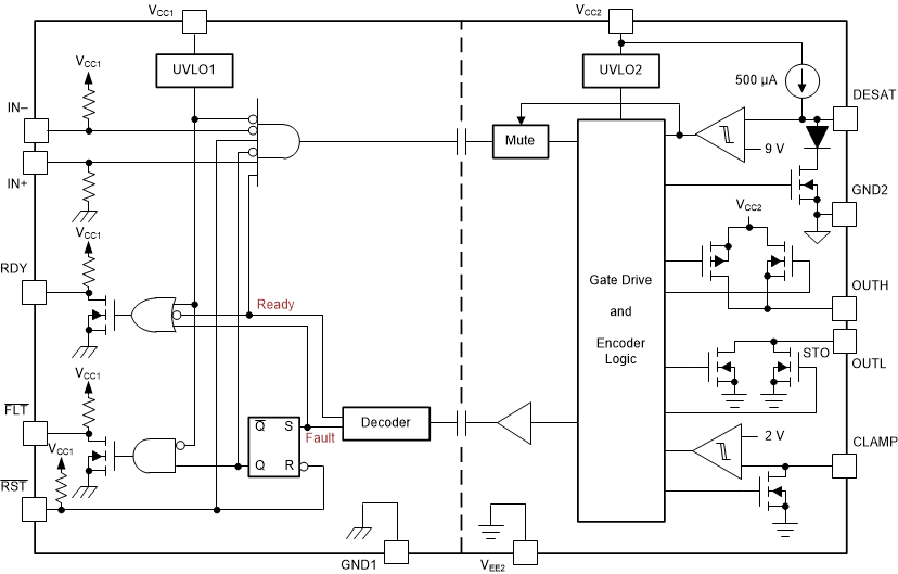
The ISO5852S and ISO5452 are isolated smart gate driver for IGBTs and MOSFETs. The input CMOS logic and output power stage are separated by a silicon dioxide (SiO2) capacitive isolation. Figure 2-9 shows the functional block diagram.
 Figure 2-9 ISO5852S, ISO5452 Functional Block Diagram
The I/O circuit on the input side interfaces with an MCU and consists of gate drive control (IN+|IN–) inputs, RESET (RST) input, READY (RDY) alarm output, and FAULT (FLT) alarm output. The power stage consists of power transistors which supply 2.5-A pullup and 5-A pulldown currents to drive the capacitive load of the external power transactions, as Well as the DESAT detection circuit to monitor the IGBT for collector-emitter overvoltage during short-circuit events. The capacitive isolation core consists of transmit circuitry to couple signals across the capacitive isolation barrier and receive the circuitry to convert the resulting low-swing signals into CMOS levels. The ISO5852S, ISO5452 also contains undervoltage lockout (UVLO) circuitry to prevent insufficient gate drive to the external IGBT. Additionally, it offers an active output pulldown feature, which ensures that the gate-driver Output is held low if the output supply voltage is absent. The ISO5852S, ISO5452 also has an active Miller clamp function which can be used to prevent parasitic turn-on of the external power transistor, due to the Miller effect, for unipolar supply operation.