TIDUF18A October 2022 – February 2024
- 1
- Description
- Resources
- Features
- Applications
- 6
- 1 CLLLC System Description
- 2 CLLLC System Overview
- 3 Totem Pole PFC System Description
- 4 Highlighted Products
-
5 Hardware, Software, Testing Requirements, and Test Results
- 5.1 Required Hardware and Software
- 5.2
Testing and Results
- 5.2.1 Test Setup (Initial)
- 5.2.2
CLLLC Test Procedure
- 5.2.2.1 Lab 1. Primary to Secondary Power Flow, Open Loop Check PWM Driver
- 5.2.2.2
Lab 2. Primary to Secondary Power Flow, Open Loop CheckPWM
Driver and ADC with Protection, Resistive Load Connected on Secondary
- 5.2.2.2.1 Setting Software Options for Lab 2
- 5.2.2.2.2 Building and Loading the Project and Setting up Debug Environment
- 5.2.2.2.3 Using Real-time Emulation
- 5.2.2.2.4 Running the Code
- 5.2.2.2.5 Measure SFRA Plant for Voltage Loop
- 5.2.2.2.6 Verify Active Synchronous Rectification
- 5.2.2.2.7 Measure SFRA Plant for Current Loop
- 5.2.2.3 Lab 3. Primary to Secondary Power Flow, Closed Voltage Loop Check, With Resistive Load Connected on Secondary
- 5.2.2.4 Lab 4. Primary to Secondary Power Flow, Closed Current Loop Check, With Resistive Load Connected on Secondary
- 5.2.2.5 Lab 5. Primary to Secondary Power Flow, Closed Current Loop Check, With Resistive Load Connected on Secondary in Parallel to a Voltage Source to Emulate a Battery Connection on Secondary Side
- 5.2.3 TTPLPFC Test procedure
- 5.2.4 Test Results
- 6 Design Files
- 7 Software Files
- 8 Related Documentation
- 9 Terminology
- 10About the Author
- 11Revision History
2.2.3 PWM Modulation
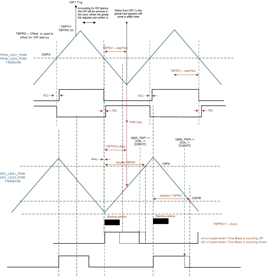
Figure 2-14 shows the PWM waveform configuration used on this design.
High-resolution PWM is used for the primary legs and the secondary legs. Up-down count mode is used to generate the PWMs. To use the high-resolution PWMs, the PRIM_LEG1_H PWM pulse is centered on the period event and the time base is configured to be up-down count. A complementary pulse with high-resolution dead time is then generated for the complementary switch. Between LEG1 and LEG2, there is a 180-degree phase shift for a full-bridge operation. This is achieved by using the feature on the PWM module to swap the xA and xB output. (Alternatively, a phase shift can also be implemented, but is not needed on this design.)
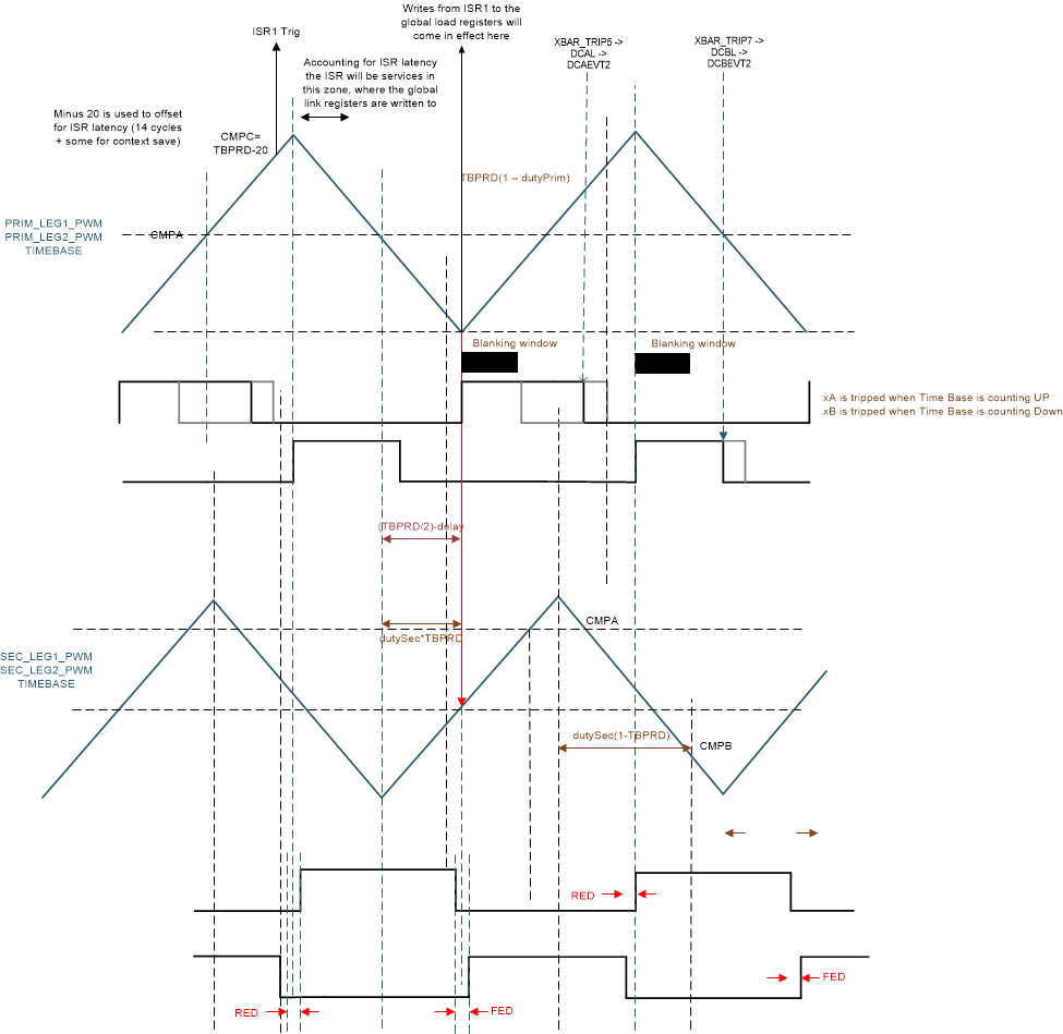
The PWM pulse to the secondary side goes through an isolator, which adds additional propagation delay. To account for this propagation delay, a small advance of the PWM is required. This is implemented in form of a phase-shift delay with respect to the primary active PWM pulse’s falling edge. The phase shift of the secondary side is a combination of the period and the delay needed for the isolator, as shown in Figure 2-14. As active synchronous rectification scheme is used, the rising edge is controlled by the primary side PWM switch timing. As the switching event can be noisy, a blanking window is used. The current in the secondary tank can be discontinuous depending on the operating frequency and load. Hence, the falling edge is controlled by the trip action that is triggered as soon as the secondary current reaches zero. The trip is then latched until the next zero or period event to avoid any spurious turn on of the secondary side switches because of noise. The blanking pulse is generated by the PWM time base but the trip latch and the blanking actions happen as part of the CMPSS. Depending on whether it is the positive half or the negative half of the tank current, two different trip signals are generated and sent to the PWM module through the X-Bar. The Type-4 PWM on the C2000 MCU can uniquely use these events to trip the xA pulse during the up count and xB during the down count. For details, refer to the code in the function CLLLC_HAL_setupSynchronousRectificationAction(), which is the HAL file for the solution, see Section 5.1.2.
The global link mechanism on the Type-4 PWM is used to reduce the number of cycles needed to update the registers and enables high-frequency operation. For example, the following code in the CLLLC_HAL_setupPWM() function links the TBPRD registers for all the PWM Legs. Using this linkage, a single write to the PRIM_LEG1 TBPRD register will write the value to PRIM_LEF2, SEC_LEG1, and SEC_LEG2.
EPWM_setupEPWMLinks(CLLLC_PRIM_LEG2_PWM_BASE,
                    EPWM_LINK_WITH_EPWM_1,
                    EPWM_LINK_TBPRD);
EPWM_setupEPWMLinks(CLLLC_SEC_LEG1_PWM_BASE,
                    EPWM_LINK_WITH_EPWM_1,
                    EPWM_LINK_TBPRD);
EPWM_setupEPWMLinks(CLLLC_SEC_LEG2_PWM_BASE,
                    EPWM_LINK_WITH_EPWM_1,
                    EPWM_LINK_TBPRD);
High-resolution PWM relies on carrying forward remainder calculation from the previous cycle into the next; hence, a periodic sync should not be used between the primary and secondary side PWMs to maintain the phase relation. Whenever a frequency change or duty change is detected, a one-time sync is issued using a fast interrupt service routine (ISR1, see Section 5.1.2.2).
 Figure 2-14 PWM Scheme Used on CLLLC Design With Active Synchronous Rectification with Power Flow Primary to Secondary
Similarly for the reverse power flow direction, the PWM configuration used is shown in Figure 2-15
 Figure 2-15 PWM Scheme Used on CLLLC Design With Active Synchronous Rectification with Power Flow Secondary to Primary