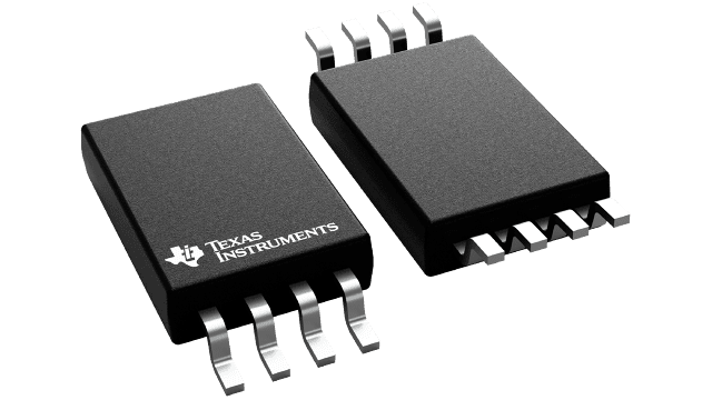
8-pin (PW) package image

CDCS503TPWRQ1 ACTIVE

Automotive clock buffer/clock multiplier with optional SSC

ACTIVE custom-reels CUSTOM Custom reel may be available

Pricing

Qty Price
+

Quality information

Rating Automotive
RoHS Yes
REACH Yes
Lead finish / Ball material NIPDAU
MSL rating / Peak reflow Level-3-260C-168 HR
Quality, reliability
& packaging information

Information included:

  • RoHS
  • REACH
  • Device marking
  • Lead finish / Ball material
  • MSL rating / Peak reflow
  • MTBF/FIT estimates
  • Material content
  • Qualification summary
  • Ongoing reliability monitoring
View or download
Additional manufacturing information

Information included:

  • Fab location
  • Assembly location
View

Export classification

*For reference only

  • US ECCN: EAR99

Packaging information

Package | Pins TSSOP (PW) | 8
Operating temperature range (°C) -40 to 105
Package qty | Carrier 2,000 | LARGE T&R

Features for the CDCS503-Q1

  • Qualified for Automotive Applications
  • AEC-Q100 Test Guidance With the Following Results:
    • Device Temperature Grade 2
    • –40°C to 105°C
      Ambient Operating Temperature Range
    • Device HBM ESD Classification Level H2
    • Device CDM ESD Classification Level C3B
  • Part of a Family of Easy to Use Clock Generator
    Devices With Optional Spread Spectrum Clocking (SSC)
  • Clock Multiplier With Selectable Output Frequency and Selectable SSC
  • SSC Controllable Through Two External Pins
    • ±0%, ±0.5%, ±1%, ±2% Center Spread
  • Frequency Multiplication Selectable Between x1 or x4 With One External Control Pin
  • Output Disable Through Control Pin
  • Single 3.3 V Device Power Supply
  • Wide Temperature Range –40°C to 105°C
  • Low Space Consumption 8-Pin TSSOP Package

Description for the CDCS503-Q1

The CDCS503-Q1 device is a spread spectrum capable, LVCMOS input clock buffer with selectable frequency multiplication.

It shares major functionality with the CDCS502 but uses a LVCMOS input stage instead of the crystal input stage of the CDCS502, and the CDCS503-Q1 has an output enable pin.

The device accepts a 3.3-V LVCMOS signal at the input.

The input signal is processed by a phased-locked loop (PLL), whose output frequency is either equal to the input frequency or multiplied by the factor of four.

The PLL is also able to spread the clock signal by ±0%, ±0.5%, ±1% or ±2% centered around the output clock frequency with a triangular modulation.

By this, the device can generate output frequencies between 8 MHz and 108 MHz with or without SSC.

A separate control pin can be used to enable or disable the output. The CDCS503-Q1 device operates in a 3.3-V environment.

It is characterized for operation from –40°C to 105°C, and available in an 8-pin TSSOP package.
Pricing

Qty Price
+

Carrier options

You can choose different carrier options based on the quantity of parts, including full reel, custom reel, cut tape, tube or tray.

A custom reel is a continuous length of cut tape from one reel to maintain lot- and date-code traceability, built to the exact quantity requested. Following industry standards, a brass shim connects an 18-inch leader and trailer on both sides of the cut tape for direct feeding into automated assembly machines. TI includes a reeling fee for custom reel orders.

Cut tape is a length of tape cut from a reel. TI may fulfill orders using multiple strips of cut tapes or boxes to satisfy the quantity requested.

TI often ships tube or tray devices inside a box or in the tube or tray, depending on inventory availability. We pack all tapes, tubes or sample boxes according to internal electrostatic discharge and moisture-sensitivity-level protection requirements.

Learn more

Lot and date code selection may be available

Add a quantity to your cart and begin the checkout process to view the options available to select lot or date codes from existing inventory.

Learn more