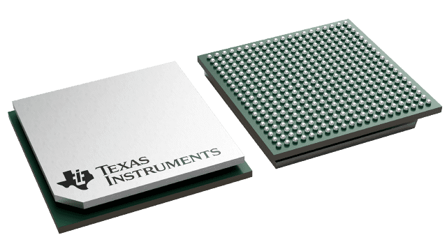
Packaging information
| Package | Pins FCBGA (ABJ) | 400 |
| Operating temperature range (°C) -40 to 85 |
| Package qty | Carrier 90 | JEDEC TRAY (5+1) |
Features for the AFE7444
- Four, 14-bit, 9-GSPS DACs
- Up to 800-MHz signal bandwidth
- 1 DSA per channel tunes output power
- Four,
14-Bit, 3-GSPS ADCs
- Up to 800-MHz signal bandwidth
- NSD: –151 dBFS/Hz
- AC performance at
fIN = 2.6 GHz, –3 dBFS
- SNR: 55 dBFS
- SFDR: 73 dBc HD2 and HD3
- SFDR: 91 dBc worst spur
- 2 DSA per channel extends dynamic range
- RF and digital power detectors
- RF frequency range: 10 MHz to 6 GHz
- Fast frequency hopping < 1 µs
- Receive digital signal
path:
- dual DDC per ADC
- 3-phase coherent 32-bit NCOs per DDC
- Decimation ratio: 3x to 32x
- Transmit digital signal
path:
- Dual DUC per DAC with 32-bit NCOs
- Interpolation ratio: 8x to 36x
- Sin(x)/x correction and configurable delay
- Power amplifier protection (PAP)
- JESD204B interface:
- 8 transceivers at up to 15 Gbps
- Subclass 1 multichip synchronization
- Clocks:
- Internal PLL and VCO with bypass option
- Clock output up to 3 GHz with clock divider
- DAC power dissipation: 1.7 W/ch at 9 GSPS
- ADC power dissipation: 1.8 W/ch at 3 GSPS
- Package: 17-mm x 17-mm FC BGA, 0.8-mm pitch
Description for the AFE7444
The AFE7444 is a quad-channel, wideband, RF-sampling analog front end (AFE) based on 14-bit, 9-GSPS DACs and 14-bit, 3-GSPS ADCs. With operation at an RF of up to 6 GHz, this device enables direct RF sampling into the C-band frequency range without the need for additional frequency conversions stages. This improvement in density and flexibility enables high-channel-count, multimission systems.
The DAC signal paths support interpolation and digital up conversion options that deliver up to 800 MHz of signal bandwidth. The differential output path includes a digital step attenuator (DSA), which enables tuning of output power.
Each ADC input path includes a dual DSA and RF and Digital power detectors. Flexible decimation options provide optimization of data bandwidth.
An 8-lane (8 TX + 8 RX) subclass-1 compliant JESD204B interface operates at up to 15 Gbps. A bypassable on-chip PLL simplifies clock operation with an optional clock output.