SBOS998D June 2021 – July 2025 BUF802
PRODUCTION DATA
- 1
- 1 Features
- 2 Applications
- 3 Description
- 4 Pin Configuration and Functions
- 5 Specifications
- 6 Parameter Measurement Information
- 7 Detailed Description
- 8 Application and Implementation
- 9 Device and Documentation Support
- 10Revision History
- 11Mechanical, Packaging, and Orderable Information
Package Options
Refer to the PDF data sheet for device specific package drawings
Mechanical Data (Package|Pins)
- RGT|16
Thermal pad, mechanical data (Package|Pins)
- RGT|16
Orderable Information
7.2 Functional Block Diagram
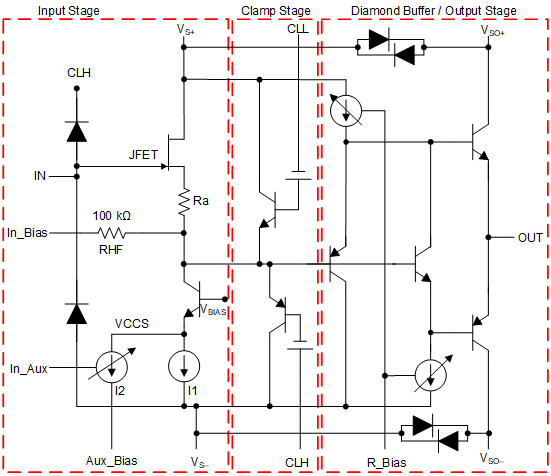
The functional block diagram shows an overview of the internal structure of the BUF802. The internal schematic of the BUF802 is divided into the following three parts:
- Input Stage: consists of a low-noise JFET with biasing circuitry. The input stage is configurable in two modes: BF Mode and CL Mode. Choosing one of the two modes affects the circuit operation of the input stage. The clamp and output stage operation are unaffected by the mode selection. Section 7.4 describes the two modes in greater detail.
- Clamp Stage: provides the
following functions:
- Protects the input of the BUF802 against large input signal transients through diode clamps to VS- and CLH respectively.
- Prevents the output voltage of the BUF802 from exceeding the voltage at the CLH and CLL.
- Output Stage: tracks the JFET source voltage and is optimized to drive 50-Ω and 100-Ω loads while maintaining signal fidelity.