SBOS998D June 2021 – July 2025 BUF802
PRODUCTION DATA
- 1
- 1 Features
- 2 Applications
- 3 Description
- 4 Pin Configuration and Functions
- 5 Specifications
- 6 Parameter Measurement Information
- 7 Detailed Description
- 8 Application and Implementation
- 9 Device and Documentation Support
- 10Revision History
- 11Mechanical, Packaging, and Orderable Information
Package Options
Refer to the PDF data sheet for device specific package drawings
Mechanical Data (Package|Pins)
- RGT|16
Thermal pad, mechanical data (Package|Pins)
- RGT|16
Orderable Information
7.4.1 Buffer Mode (BF Mode)
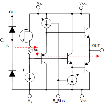
 Figure 7-9 Internal Schematic – BF
Mode
Figure 7-9 Internal Schematic – BF
ModeThe wide large-signal bandwidth and fast slew rate of the BUF802 coupled with Hi-Z input are useful in a variety of high-frequency signal chain applications. Figure 7-9 shows that the BUF802 uses the Main Path and operates the JFET and transistors as source follower and emitter followers to reproduce signal applied on IN, at the output of BUF802. The pins associated with only CL Mode (Pin No. 6, 4, and 3) are left floating while operating in BF Mode.
 Figure 7-10 Composite Loop Using BF
Mode
Figure 7-10 Composite Loop Using BF
ModeFigure 7-10 shows how the BUF802 is also used in a composite loop while being operated in BF Mode. The operation of BUF802 in Figure 7-10 is still called BF Mode because the signal is being transferred through the Main Path only. The Auxiliary path and the pins associated with the Auxiliary path and CL Mode are kept disabled. The low-frequency and high-frequency signal components are combined externally through the discrete components R1 and C1 before being applied at the IN pin.