SBOS998D June 2021 – July 2025 BUF802
PRODUCTION DATA
- 1
- 1 Features
- 2 Applications
- 3 Description
- 4 Pin Configuration and Functions
- 5 Specifications
- 6 Parameter Measurement Information
- 7 Detailed Description
- 8 Application and Implementation
- 9 Device and Documentation Support
- 10Revision History
- 11Mechanical, Packaging, and Orderable Information
Package Options
Refer to the PDF data sheet for device specific package drawings
Mechanical Data (Package|Pins)
- RGT|16
Thermal pad, mechanical data (Package|Pins)
- RGT|16
Orderable Information
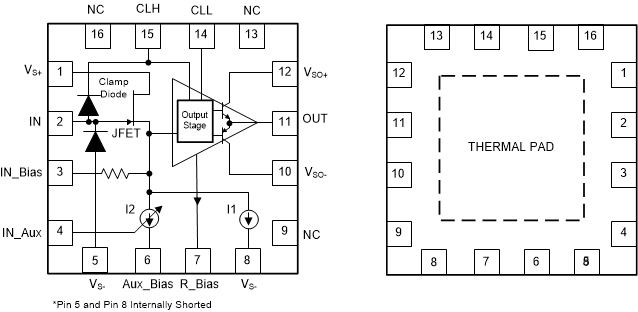
4 Pin Configuration and Functions
 Figure 4-1 RGT Package, 16-Pin VQFN
(Top View and Bottom View)
Table 4-1 Pin Functions
| PIN | TYPE(1) | OPERATING MODE(2)(3) | DESCRIPTION | |
|---|---|---|---|---|
| NAME | NO. | |||
| Aux_Bias | 6 | P | CL | Connect to VS– to enable control of OUT through the In_Aux |
| CLH | 15 | I | BF, CL | Input pin for setting positive clamp voltage |
| CLL | 14 | I | BF, CL | Input pin for setting negative clamp voltage |
| IN | 2 | I | BF, CL | Signal input |
| In_Aux | 4 | I | CL | Auxiliary input for controlling OUT through an external amplifier |
| In_Bias | 3 | I | CL | JFET biasing pin |
| NC | 16, 13, 9 | NC | — | Do not connect |
| OUT | 11 | O | BF, CL | Signal output |
| R_Bias | 7 | I | BF, CL | Output-stage bias-current setting pin |
| VS+ | 1 | P | BF, CL | Positive power supply connection for the input stage |
| VS– | 5, 8 | P | BF, CL | Negative power supply connection for the input stage; pin 5 and pin 8 are internally shorted |
| VSO+(4) | 12 | P | BF, CL | Positive power supply connection for the output stage |
| VSO–(4) | 10 | P | BF, CL | Negative power supply connection for the output stag |
| Thermal Pad | — | — | The thermal pad is electrically isolated from the die and pins; connect the thermal pad to any potential | |
(1) I = input, O= output, P= power, NC = no connect.
(2) See Section 7.4 for more information on Buffer Mode (BF) and
Composite Loop Mode (CL) functional modes.
(3) Use pins specified as CL only when operating in
Composite Loop Mode, and float these pins when operating in Buffer
Mode.
(4) Tie VSO and VS to the same potential
because these pins are internally connected to the other through back-to-back
diodes.