DLPS206 May 2021 DLPC7540
PRODUCTION DATA
- 1 Features
- 2 Applications
- 3 Description
- 4 Revision History
- 5 Pin Configuration and Functions
-
6 Specifications
- 6.1 Absolute Maximum Ratings
- 6.2 ESD Ratings
- 6.3 Recommended Operating Conditions
- 6.4 Thermal Information
- 6.5 Power Electrical Characteristics
- 6.6 Pin Electrical Characteristics
- 6.7 DMD HSSI Electrical Characteristics
- 6.8 DMD Low-Speed LVDS Electrical Characteristics
- 6.9 V-by-One Interface Electrical Characteristics
- 6.10 FPD-Link LVDS Electrical Characteristics
- 6.11 USB Electrical Characteristics
- 6.12 System Oscillator Timing Requirements
- 6.13 Power Supply and Reset Timing Requirements
- 6.14 DMD HSSI Timing Requirements
- 6.15 DMD Low-Speed LVDS Timing Requirements
- 6.16 V-by-One Interface General Timing Requirements
- 6.17 FPD-Link Interface General Timing Requirements
- 6.18 Source Frame Timing Requirements
- 6.19 Synchronous Serial Port Interface Timing Requirements
- 6.20 Master and Slave I2C Interface Timing Requirements
- 6.21 Programmable Output Clock Timing Requirements
- 6.22 JTAG Boundary Scan Interface Timing Requirements (Debug Only)
- 6.23 JTAG ARM Multi-Ice Interface Timing Requirements (Debug Only)
- 6.24 Multi-Trace ETM Interface Timing Requirements
- 7 Detailed Description
- 8 Application and Implementation
- 9 Power Supply Recommendations
-
10Layout
- 10.1
Layout Guidelines
- 10.1.1 General Layout Guidelines
- 10.1.2 Power Supply Layout Guidelines
- 10.1.3 Layout Guidelines for Internal Controller PLL Power
- 10.1.4 Layout Guideline for DLPC7540 Reference Clock
- 10.1.5 V-by-One Interface Layout Considerations
- 10.1.6 FPD-Link Interface Layout Considerations
- 10.1.7 USB Interface Layout Considerations
- 10.1.8 DMD Interface Layout Considerations
- 10.1.9 General Handling Guidelines for Unused CMOS-Type Pins
- 10.1.10 Maximum Pin-to-Pin, PCB Interconnects Etch Lengths
- 10.2 Thermal Considerations
- 10.1
Layout Guidelines
- 11Device and Documentation Support
- 12Mechanical, Packaging, and Orderable Information
Package Options
Mechanical Data (Package|Pins)
- ZDC|676
Thermal pad, mechanical data (Package|Pins)
Orderable Information
3 Description
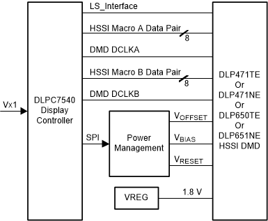
The DLPC7540 is a digital display controller for the 4K UHD and 1080p display chipsets, which comprises of DLPC7540 controller, DLP471TE, DLP471NE, DLP650TE or DLP651NE DMDs and DLPA100 Power and Motor driver. This solution targets display systems that require high resolution and high brightness in a small form factor. To ensure reliable operation, the DLPC7540 controller must always be used with the DLP471TE, DLP471NE, DLP650TE or DLP651NE DMDs and the DLPA100 power management integrated circuit in each application.
Device Information(1)(2)
| PART NUMBER | PACKAGE | BODY SIZE (NOM) |
|---|---|---|
| DLPC7540ZDC | P-HBGA (676) | 31.00 mm × 31.00 mm |
(1) For all available packages, see the orderable addendum.
(2) Includes embedded heat slug.
 Figure 3-1 Typical Standalone
System