SLVSEE9D April 2020 – April 2021 DRV8889-Q1
PRODUCTION DATA
- 1 Features
- 2 Applications
- 3 Description
- 4 Revision History
- 5 Pin Configuration and Functions
- 6 Specifications
-
7 Detailed Description
- 7.1 Overview
- 7.2 Functional Block Diagram
- 7.3
Feature Description
- 7.3.1 Stepper Motor Driver Current Ratings
- 7.3.2 PWM Motor Drivers
- 7.3.3 Microstepping Indexer
- 7.3.4 Controlling VREF with an MCU DAC
- 7.3.5 Current Regulation
- 7.3.6
Decay Modes
- 7.3.6.1 Slow Decay for Increasing and Decreasing Current
- 7.3.6.2 Slow Decay for Increasing Current, Mixed Decay for Decreasing Current
- 7.3.6.3 Mode 4: Slow Decay for Increasing Current, Fast Decay for Decreasing current
- 7.3.6.4 Mixed Decay for Increasing and Decreasing Current
- 7.3.6.5 Smart tune Dynamic Decay
- 7.3.6.6 Smart tune Ripple Control
- 7.3.7 Blanking Time
- 7.3.8 Charge Pump
- 7.3.9 Linear Voltage Regulators
- 7.3.10 Logic Level Pin Diagrams
- 7.3.11 Protection Circuits
- 7.4 Device Functional Modes
- 7.5 Programming
- 7.6 Register Maps
-
8 Application and Implementation
- 8.1 Application Information
- 8.2 Typical Application
- 9 Power Supply Recommendations
- 10Layout
- 11Device and Documentation Support
- 12Mechanical, Packaging, and Orderable Information
Package Options
Mechanical Data (Package|Pins)
Thermal pad, mechanical data (Package|Pins)
Orderable Information
8.2.4.4 Thermal Parameters for VQFN Package
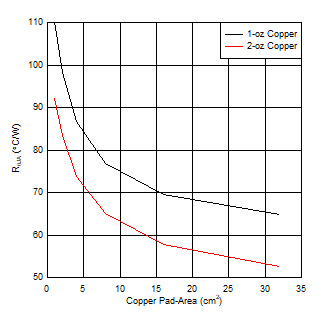
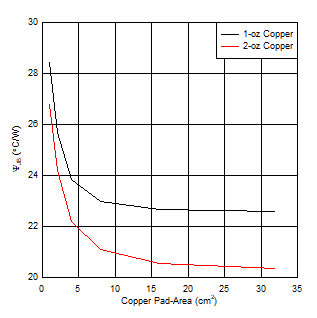
Figure 8-19 and Figure 8-20 show the variation of the RθJA (Junction-to-Ambient Thermal Resistance) and ΨJB (Junction-to-Board Characterization Parameter) with copper-pad area for 2-layer PCB, for the VQFN package. As shown in these curves, the thermal resistance is lower for the higher copper thickness PCB and the higher copper pad-area.
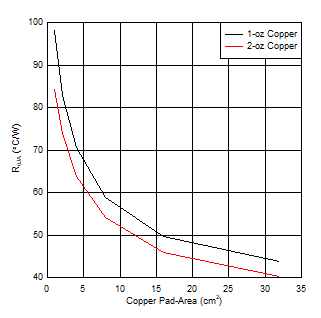
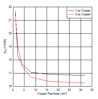
Similarly, Figure 8-21 and Figure 8-22 show the variation of the RθJA and ΨJB with copper-pad area for 4-layer PCB respectively, for the VQFN package.
The thermal parameters (RθJA (Junction-to-Ambient Thermal Resistance) and ΨJB (Junction-to-Board Characterization Parameter)) are calculated considering the ambient temperature of 25°C and with 2-W power evenly dissipated between high-side and low-side FET's. The thermal parameters calculated considering the power dissipation at the actual location of the power-FETs rather than an averaged estimation.
The thermal parameters are highly dependent on the external conditions such as altitude, package geometry etc. Refer to Application Report for more details.
 Figure 8-19 2-Layer PCB Junction-to-Ambient Thermal Resistance (RθJA) vs Copper Area
 Figure 8-21 4-Layer PCB Junction-to-Ambient Thermal Resistance (RθJA) vs Copper Area
 Figure 8-20 2-Layer PCB Junction-to-Board Characterization Parameter (ΨJB) vs Copper Area
 Figure 8-22 4-Layer PCB Junction-to-Board Characterization (ΨJB) Parameter vs Copper Area