SLVSEE9D April 2020 – April 2021 DRV8889-Q1
PRODUCTION DATA
- 1 Features
- 2 Applications
- 3 Description
- 4 Revision History
- 5 Pin Configuration and Functions
- 6 Specifications
-
7 Detailed Description
- 7.1 Overview
- 7.2 Functional Block Diagram
- 7.3
Feature Description
- 7.3.1 Stepper Motor Driver Current Ratings
- 7.3.2 PWM Motor Drivers
- 7.3.3 Microstepping Indexer
- 7.3.4 Controlling VREF with an MCU DAC
- 7.3.5 Current Regulation
- 7.3.6
Decay Modes
- 7.3.6.1 Slow Decay for Increasing and Decreasing Current
- 7.3.6.2 Slow Decay for Increasing Current, Mixed Decay for Decreasing Current
- 7.3.6.3 Mode 4: Slow Decay for Increasing Current, Fast Decay for Decreasing current
- 7.3.6.4 Mixed Decay for Increasing and Decreasing Current
- 7.3.6.5 Smart tune Dynamic Decay
- 7.3.6.6 Smart tune Ripple Control
- 7.3.7 Blanking Time
- 7.3.8 Charge Pump
- 7.3.9 Linear Voltage Regulators
- 7.3.10 Logic Level Pin Diagrams
- 7.3.11 Protection Circuits
- 7.4 Device Functional Modes
- 7.5 Programming
- 7.6 Register Maps
-
8 Application and Implementation
- 8.1 Application Information
- 8.2 Typical Application
- 9 Power Supply Recommendations
- 10Layout
- 11Device and Documentation Support
- 12Mechanical, Packaging, and Orderable Information
Package Options
Mechanical Data (Package|Pins)
Thermal pad, mechanical data (Package|Pins)
Orderable Information
3 Description
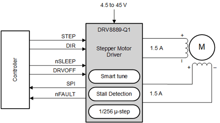
The DRV8889-Q1 and DRV8889A-Q1 are fully integrated stepper motor drivers, supporting up to 1.5 A full scale current with an internal microstepping indexer, smart tune decay technology, advanced stall detection algorithm, and integrated current sensing.
The device supports up to 1/256 levels of microstepping to enable a smooth motion profile. Integrated current sensing eliminates the need for two external resistors, saving board space and cost. With advanced stall detection algorithm, designers can detect if the motor stopped and take action as needed which can improve efficiency and reduce noise. The device provides 8 decay mode options including: smart tune, slow, and mixed decay options. Smart tune automatically adjusts for optimal current regulation performance. The device also includes an integrated torque DAC which allows for the controller to scale the output current through SPI without needing to scale the VREF voltage reference. A low-power sleep mode is provided using an nSLEEP pin. The device features full duplex, 4-wire synchronous SPI communication, with daisy chain support for up to 63 devices connected in series, for configurability and detailed fault reporting. View our full portfolio of stepper motor drivers on ti.com.
| PART NUMBER (1) | PACKAGE | BODY SIZE (NOM) |
|---|---|---|
| DRV8889QPWPRQ1 | HTSSOP (24) | 7.80 mm × 4.40 mm |
| DRV8889QWRGERQ1 | VQFN (24) (Wettable Flank) | 4.00 mm × 4.00 mm |
| DRV8889AQPWPRQ1 | HTSSOP (24) | 7.80 mm × 4.40 mm |
| DRV8889AQWRGERQ1 | VQFN (24) (Wettable Flank) | 4.00 mm × 4.00 mm |
 Simplified Schematic